 Neditek

PACKAGED GaAs MMIC POWER AMPLIFIER
1 Watt RF Power Amplifier
Model: NDGB020004
The neditek NDGB020004 is a packaged GaAs MMIC that delivers 1 W at P1dB from 0.7 to 2.7 GHz. Its 22.5 dB gain, 37 dBm OIP3, 5 V supply and compact QFN 4 × 4 mm package suit broadband driver stages, radio transmitters and RF test platforms.
- Frequency range0.7–2.7 GHz
- Linear output30 dBm at P1dB
- Power gain22.5 dB
- Supply5 V
- PackageQFN 4 × 4 mm, 20 leads
- Standard MOQ10 pcs
OUTPUT DEFINITION
1 W At P1dB Provides A Clear Linear Output Target
A 1 W label can refer to saturation, a compression point or an average operating level, and those definitions produce different link budgets.
| Power reference | What it means for selection |
|---|---|
| P1dB: 30 dBm | The stated 1 W point is the output where small-signal gain has compressed by 1 dB. |
| Modulated operation | Waveform-specific back-off controls distortion and spectral regrowth. |
Buyer takeaway: NDGB020004 reaches 30 dBm at P1dB, so 1 W is the defined compression-point output rather than an unspecified peak value.
BAND COVERAGE DECISION
0.7–2.7 GHz Coverage Supports Fewer Driver Variants
A wide tuning range can reduce hardware variants only when gain, match and stability are verified at the band edges as well as the center.
Shared Hardware Benefit
One qualified driver design can serve multiple sub-bands and reduce separate amplifier inventory.
Qualification Condition
Qualification covers output, gain, input and output match, and stability at 0.7 GHz, 2.7 GHz and the intended channels.
Discard Condition
A narrow fixed-band design gains little from shared wideband hardware if a tuned device offers a better system tradeoff.
Buyer takeaway: NDGB020004 covers 0.7–2.7 GHz with 22.5 dB gain, making it suitable for multi-band driver stages that are qualified across the full operating band.
PCB INTEGRATION
5 V QFN Integration Depends On Grounding And Heat Flow
A 4 × 4 mm QFN package shortens RF interconnects, but its exposed ground and thermal path become part of the amplifier circuit.
Continuous Exposed Pad
A low-inductance pad connection supports RF return current and moves heat into the board.
Dense Ground Vias
Closely spaced vias reduce return-path inductance and thermal resistance beneath the package.
Separated RF Paths
Short controlled-impedance traces and physical input-output separation reduce unwanted feedback.
Buyer takeaway: A continuous ground pad, dense vias, local decoupling and separated input/output routes protect gain stability while carrying heat into the PCB.
COMPLETE SPECIFICATIONS
NDGB020004 Ordering And Interface Data
The purchase specification combines the electrical ratings with the package and traceability requirements.
| Product Name | 1 Watt RF Power Amplifier |
|---|---|
| Model / Part Number | NDGB020004 |
| Product Category | Packaged GaAs MMIC Power Amplifier |
| Frequency Range | 0.7–2.7 GHz |
| Linear Output | 30 dBm at P1dB |
| Power Gain | 22.5 dB |
| OIP3 / Noise Figure | 37 dBm / 6.4 dB |
| Supply / Maximum RF Input | 5 V / 15 dBm |
| Package And Interface | QFN 4 × 4 mm, 20 leads; 50 Ω RF input/output; exposed ground and thermal pad |
| Marking And Packaging | Part and lot traceability; antistatic tape-and-reel in moisture-barrier dry pack |
APPLICATIONS & EQUIPMENT
Where NDGB020004 Fits The Signal Chain
Final equipment fit depends on the operating sub-band, waveform back-off, filtering and load match.
Broadband Driver Stage
A 0.7–2.7 GHz driver stage can precede a higher-power final stage when output back-off and interstage matching are verified.
UHF And L-Band Transmitters
The device fits telemetry, land-mobile and industrial radio transmit paths whose sub-band, filtering and linearity targets fall inside the rated range.
RF Test And Instrumentation
The model provides a compact broadband gain block for calibrated RF stimulus after band-edge gain and match are qualified.
MATERIALS & MANUFACTURING
GaAs Construction Supports The RF Signal Path
The material stack combines a semi-insulating substrate with conductive metallization and surface passivation.
Substrate
Semi-insulating GaAs supports microwave device isolation and compact MMIC integration.
Metallization
Multi-layer gold metallization forms the RF interconnect and device contacts.
Passivation
Silicon-nitride and glass passivation protect the active device surface before QFN packaging.
PERFORMANCE & WORKING CONDITIONS
The RF Operating Window Before Layout Freeze
The published ratings set the model-selection baseline; final-board qualification covers temperature, match and waveform back-off.
RF Path
A 50 Ω signal path covers 0.7–2.7 GHz.
Temperature
The design target is −40 °C to +85 °C; the ordered screening level remains subject to quotation.
Electrical Limits
The limits are a 5 V supply, maximum RF input of 15 dBm and nominal load VSWR ≤ 2:1.
Board Conditions
A solid exposed-pad ground, dense thermal vias, local decoupling and separated RF input/output routes support stable operation.
CUSTOMIZATION
Order-Specific Screening And Delivery Details
The inquiry establishes the required band, test points, traceability and packing configuration.
- Electrical Screening
Frequency points, power, gain and temperature coverage are defined with the order. - Band-Specific Evaluation
Additional checks can cover the intended channel or band edges. - Marking And Traceability
Part marking, lot label and shipment records follow the approved order.
- Tape-And-Reel Configuration
Reel quantity, orientation and dry-pack requirements are order-specific. - Evaluation Board And Data Package
An evaluation fixture and application data can support design-in work. - Custom Order Threshold
Engineering changes normally start from 100 pcs and require 6–10 weeks after specification freeze.
USE & SAFETY INSTRUCTIONS
Mount And Start The QFN Amplifier In A Controlled Sequence
Use the approved land pattern, an ESD-safe work area and instrumented startup before applying full RF drive.
Receiving And ESD Inspection
Keep devices in ESD-safe handling. Check the dry-pack indicator, reel label and part number before opening or mounting.
QFN Mounting And RF Layout
Use the approved QFN4×4_20L land pattern. Connect the exposed pad continuously to ground and add dense vias into the PCB thermal plane.
Controlled Startup And RF Drive
Terminate both ports in 50 Ω, apply the specified bias sequence, confirm quiescent current, then increase RF drive gradually while monitoring temperature and output.
Storage, Reflow And Rework
Keep unused parts sealed in dry pack. Follow the approved moisture-sensitivity and reflow profile; limit rework heat and package stress.
PURCHASING CONDITIONS
Sample And Production Terms For NDGB020004
Commercial values are planning defaults and are confirmed in the final quotation.
- MOQ10 pcs standard MOQ
- Sample PolicyPaid sample available from 1 pc
- Sample Lead Time7–10 business days
- Production Lead Time4–6 weeks
- Price BasisEXW; quantity and screening dependent
- PackagingAntistatic tape-and-reel, moisture-barrier dry pack
- PaymentT/T, 50% deposit and 50% before shipment
- ShippingExpress courier or buyer-nominated freight account
PRE-SALES & AFTER-SALES SERVICE
Support From RF Selection To Delivered-Lot Review
Measured conditions and board details allow the response to address the actual design state.
Frequency And Power Review
The review covers band, drive, output definition, modulation and PCB interface before selection.
Sample And Production Records
Screening points, part marking, reel quantity and shipment documentation align with the approved order.
Application Troubleshooting
Layout, bias and measured-condition details support technical review and failure-analysis intake.
FACTORY & MANUFACTURER
Ntesy Technology Company Limited Manufactures And Supports NDGB020004
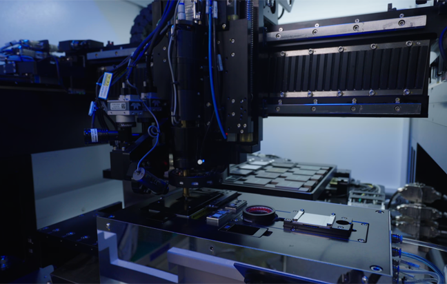
The named manufacturer in Nanjing supports the packaged GaAs amplifier from product review through order documentation.
Manufacturing And Order Support
- GaAs RF component production and packaged-device support
- RF parameter testing for frequency, power, gain and OIP3
- Lot marking, tape-and-reel packaging and export documentation
- Order-specific screening and design-in support
REQUEST A TECHNICAL QUOTE
Quote Inputs: Band, Equipment And Quantity
- Phone: 86-25-86858581
- Email: sales@neditek.com
- WhatsApp: 86-25-86858581
- Address: Room 2105, Building 1, Zichen Plaza, Gulou District, Nanjing, Jiangsu, China