 Neditek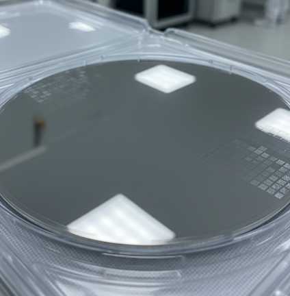
INDUSTRIAL-GRADE POWER SEMICONDUCTORS
1700V SiC MOSFET
Part Numbers: NDS010082, NDS010083, NDS010084, NDS010159, NDS010160, NDS010161, NDS010162
NEDITEK 1700V SiC MOSFETs are N-channel power switches for high-voltage industrial drives, renewable-energy converters, rail power, charging equipment, UPS systems and auxiliary power supplies. Seven industrial-grade part numbers cover 20–900 mΩ, 6–133 A, TO-247-3, TO-247-4 and TO-263-7 packages, with a 175 °C maximum junction temperature. Select by conduction loss, gate charge, thermal dissipation and board isolation requirements.
- Drain-Source Voltage1700 V
- On-Resistance20–900 mΩ
- Drain Current At 25 °C6–133 A
- Package OptionsTO-247-3, TO-247-4, TO-263-7
- Maximum Junction Temperature175 °C
- MOQ10 Pieces Per Part Number
DEVICE SELECTION
Choose The Package And Resistance Range
Lower on-resistance supports more current but increases gate charge and driver energy. Package choice changes assembly, Kelvin-source access, creepage and thermal integration.
| Part Number | Package | RDS(on) | ID At 25 °C | Total Qg | PTOT | Recommended Fit |
|---|---|---|---|---|---|---|
| NDS010082 | TO-247-4 | 20 mΩ | 133 A | 362 nC | 714 W | Higher-current converters where conduction loss is the priority |
| NDS010083 | TO-247-4 | 40 mΩ | 60 A | 142 nC | 357 W | Balanced current, drive charge and thermal load |
| NDS010084 | TO-247-4 | 80 mΩ | 37 A | 71.2 nC | 250 W | Moderate current with lower gate-drive energy |
| NDS010159 | TO-247-3 | 450 mΩ | 10 A | 15 nC | 87 W | Through-hole auxiliary or lower-current power stage |
| NDS010160 | TO-247-3 | 900 mΩ | 6 A | 6 nC | 83 W | Lowest gate charge for lower-current through-hole stages |
| NDS010161 | TO-263-7 | 450 mΩ | 10 A | 15 nC | 87 W | Surface-mount auxiliary or lower-current power stage |
| NDS010162 | TO-263-7 | 900 mΩ | 6 A | 6 nC | 83 W | Lowest gate charge for lower-current surface-mount stages |
Start with the lowest-resistance part that meets the thermal budget, then verify switching loss and gate-drive power. Use TO-247-4 when Kelvin-source control and higher current matter, TO-247-3 for conventional through-hole assembly, or TO-263-7 for a surface-mount lower-current stage.
PRODUCT PHOTOS
Review The Supplied SiC Wafer Images
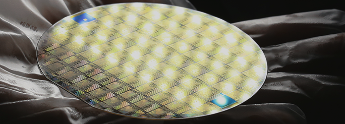
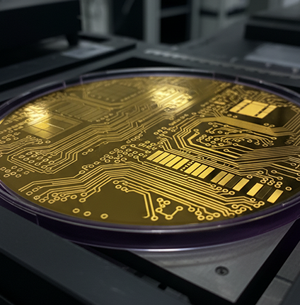
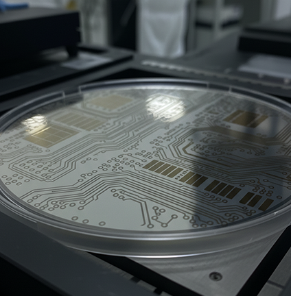
The gallery shows patterned and metallized semiconductor wafers during clean handling and fabrication-related processing.
COMPLETE SPECIFICATIONS
Compare The 1700V Series At A Glance
Ratings are series values at the stated 25 °C reference where applicable. Use the exact part-number data for loss, drive and thermal calculations.
| Product Series | 1700V SiC MOSFET Industrial Series |
|---|---|
| Part Numbers | NDS010082, NDS010083, NDS010084, NDS010159, NDS010160, NDS010161, NDS010162 |
| Device Type | N-Channel Silicon Carbide Power MOSFET |
| Drain-Source Voltage | 1700 V |
| On-Resistance At 25 °C | 20, 40, 80, 450 Or 900 mΩ By Part Number |
| Continuous Drain Current At 25 °C | 6–133 A By Part Number |
| Package Options | TO-247-3, TO-247-4 And TO-263-7 |
| Gate Threshold Voltage, Typical | 2.7–3.0 V |
| Total Gate Charge | 6–362 nC By Part Number |
| Maximum Junction Temperature | 175 °C |
APPLICATIONS & EQUIPMENT
Match The Device To The Converter
Use the 1700 V class only after the bus, overshoot, isolation and thermal requirements justify it; then choose current, resistance, gate charge and package as one system decision.
Industrial Motor Drives
Use 20–80 mΩ TO-247-4 devices where higher phase current and Kelvin-source switching control are priorities; validate DC-link overshoot, cooling and short-circuit protection in the target inverter.
Renewable Energy, Storage And UPS
Use the 1700 V rating for higher-voltage DC links that need more blocking margin than 1200 V devices. Select the resistance and gate charge together so conduction and switching losses fit the thermal budget.
Charging, Rail And Auxiliary Power
Choose TO-247-3 for conventional through-hole assembly or TO-263-7 for surface-mount lower-current stages. Verify isolation, creepage, gate-drive CMTI and dv/dt before release.
PACKAGE & TECHNICAL DATA
Use The Correct Package Reference
The NEDITEK Power Device Selection Guide maps each 1700 V part number to its package. Complete PCB and mechanical approval uses the exact package drawing for that part number.
Package Choice Changes The Power Loop
TO-247-3 provides a conventional three-lead through-hole interface, TO-247-4 adds a Kelvin source for the gate-drive return, and TO-263-7 supports surface-mount assembly. Use the exact part-number package drawing for PCB footprint, creepage, clearance and heatsink approval.
- TO-247-4 for Kelvin-source gate-drive return and higher-current devices
- TO-247-3 for conventional through-hole lower-current stages
- TO-263-7 for surface-mount lower-current stages
- Approve footprint, isolation and thermal interface against the exact part number
MATERIALS & MANUFACTURING
Understand The Device And Package Build
Material, wafer processing and package assembly determine electrical, thermal and handling behavior. Final approval remains tied to the exact part number.
Silicon Carbide Die
Vertical SiC power MOSFET die provides the controlled source-to-drain switching path and 1700 V blocking class.
Wafer To Final Test
Epitaxy, wafer fabrication, metallization, package assembly and final electrical test support the discrete-device supply chain.
Passivation And Terminations
A passivated die surface, metal power terminals and molded package body support semiconductor assembly and circuit mounting.
PERFORMANCE & WORKING CONDITIONS
Set The Electrical And Thermal Window
The 25 °C table ratings are selection references. Final limits depend on junction temperature, switching conditions, gate drive, parasitics, insulation and cooling.
CONFIGURATION & PROGRAM SUPPORT
Define The Part, Package And Approval Plan
Standard part-number selection is the primary route. Use program support to align samples, documents, lot identification and scheduled volume supply.
- Part-Number Selection: Choose 20, 40, 80, 450 Or 900 mΩ Against Current, Gate Charge And Thermal Limits.
- Package Selection: TO-247-3, TO-247-4 Or TO-263-7 To Match Through-Hole, Kelvin-Source Or Surface-Mount Assembly.
- Qualification Samples: 1–5 Pieces Per Selected Part Number For Electrical, Double-Pulse And Thermal Evaluation.
- Lot Identification: Part-Number, Lot And Packing Labels Can Be Aligned With Incoming-Inspection Records.
- Design-In Support: Review The DC Link, Topology, Gate Drive, Cooling And Protection Before Sample Approval.
- Volume Planning: Standard Lots Start At 10 Pieces Per Part Number; Larger Forecasts Can Use Scheduled Releases.
USE & SAFETY INSTRUCTIONS
Validate The Device In The Target Converter
Use the exact part-number datasheet and measured waveforms for gate-drive, switching, thermal and protection limits.
Select And Derate
Calculate The Maximum Normal, Regenerative, Switching-Overshoot And Fault Voltage. Use 1700 V As The Absolute Drain-Source Rating, Then keep the design below it with margin set by topology, layout, altitude and insulation coordination.
Validate The Gate Drive
Use The Recommended Gate-Voltage Range For The Exact Part Number. Set Separate Turn-On And Turn-Off Resistance When Needed, and verify dv/dt, di/dt, overshoot, ringing and Miller turn-on with double-pulse testing.
Control Layout And Protection
Keep The Power Loop And Gate Loop Short. Use The Kelvin Source On TO-247-4 Devices For The Driver Return, preserve creepage and clearance, and coordinate overcurrent detection, blanking and soft turn-off with the device limit.
Manage Heat, ESD And Storage
Handle Devices At A Grounded ESD Workstation, retain protective packing until assembly, mount the package to a validated thermal path and calculate peak junction temperature from the mission-profile losses rather than the 25 °C rating alone.
PURCHASING CONDITIONS
Plan Samples And Production Lots
Quote the exact part number, quantity, evaluation schedule, packing requirement and delivery destination.
- MOQ10 Pieces Per Standard Part Number
- Sample Policy1–5 Paid Evaluation Samples Per Selected Part Number
- Sample Lead Time5–7 Business Days For Available Standard Samples
- Bulk Lead Time20–30 Business Days After Sample And Order Approval
- Price BasisEXW Or FOB Quote By Exact Part Number, Quantity And Delivery Schedule
- PackagingESD-Safe Tubes Or Trays In Antistatic Barrier Packaging And Export Carton
- Payment TermsT/T, 50% Deposit And 50% Before Shipment For Production Orders
- Shipping SupportCourier Or Air For Samples; Air Or Sea Freight For Volume Lots
PRE-SALES & AFTER-SALES SERVICE
Support The Device From Selection To Repeat Supply
The workflow connects the electrical decision, sample approval and repeat-order record to the same part number.
Before Ordering
Review the DC-link voltage, current waveform, switching frequency, gate drive, package, thermal path and protection; then match the part number and sample plan.
During Production
Confirm the approved part number, quantity, lot identification, packing method and shipping documents before release.
After Delivery
Support switching-waveform, gate-drive, layout and thermal review, failure-analysis intake and repeat-order planning.
FACTORY & MANUFACTURER
NEDITEK Power-Semiconductor Supply Support
Ntesy Technology Company Limited supplies NEDITEK power-semiconductor products from Nanjing, Jiangsu Province, China.

From Wafer Processing To System Integration
NEDITEK supports epitaxy and material growth, chip design, wafer processing, package and test, quality control, module application and system integration for power-electronics programs.
- Epitaxy, material growth and wafer processing
- Chip design, package assembly and electrical test
- Quality control and lot-identification support
- Module application, design-in and export-document support
QUALITY EVIDENCE
Align The Qualification File With The Part Number
Use part-number and lot-specific records for supplier approval. The available quality-control framework covers wafer electrical test, final screening, SPC/CPK process control, material-lot verification and traceability.
- Wafer Electrical Test RecordsElectrical screening input
- Final Electrical ScreeningPart-number release record
- Online SPC And CPK Process RecordsProcess-control evidence
- Material Lot VerificationIncoming material evidence
- Part-Number And Lot TraceabilityReceiving and repeat-order reference
REQUEST A TECHNICAL QUOTE
Send The Part Number And Converter Conditions
Include the DC-link voltage, peak and RMS current, switching frequency, gate-drive plan, package, annual quantity and required qualification documents.
- Phone: +86-25-86858581
- Email: sales@neditek.com
- WhatsApp: +86-25-86858581
- Address: 524 Zhongshan East Road, Nanjing, Jiangsu Province, China