 Neditek
GaN HEMT Devices Outperforming Legacy HEMT GaN Solutions
The new generation of GaN (gallium nitride) HEMT devices have fully surpassed traditional solutions in performance. They not only completely solve the problem of dynamic on-resistance degradation, but also can continuously provide stable power added efficiency (PAE) in the high frequency band above 28 GHz. In the past, the old heterojunction structure always can not escape the surface and buffer layer “electron trap” spell, resulting in equipment under high intensity continuous wave (CW) operation, RF power will appear serious attenuation. Today, as long as the engineer in charge of selection measures the epitaxial design of modern GaN-on-SiC (silicon carbide based gallium nitride), he will immediately find that the power curve has become very flat and the junction thermal resistance has also dropped significantly. This article will break down the core differences between these advanced GaN platforms and their old silicon-based predecessor products in detail-covering specific substrate improvements, packaging mechanisms, and thermal indicators, so as to provide your R & D department with the detailed data needed for device upgrades.
Core Defects Of Conventional HEMT GaN Architecture
The power density and switching frequency of the older generation of GaN transistors are severely constrained by their own structural bottlenecks. In early products, due to the poor design of the buffer layer, once in the high drain bias state, electrons will escape from the two-dimensional electron gas (2DEG) channel.
Completely Eliminate Current Collapse And Trap Effect
Advanced GaN HEMT devices cleverly use carbon-doped or iron-doped buffer layers to neutralize deep-level traps, thus solving the current collapse phenomenon in one fell swoop. After traditional devices undergo high-voltage switching, their dynamic on-resistance (R_DS(on)) usually soars by 15% to 20%, which directly reduces the linearity of the output power. In contrast, modern fabrication processes passivate the surface states with an optimized silicon nitride (SiNx) dielectric layer. When R & D engineers perform pulse I-V measurements, they will find that in these new iterations, the dispersion between the static bias point and the active RF state is almost zero.
GaN-on-SiC Vs. Backward Substrate Options
Silicon carbide (SiC) substrates conduct heat almost three times faster than conventional silicon substrates, a feature that has fundamentally reshaped the thermal budget of RF power amplifiers. Although the price of traditional silicon-based gallium nitride (GaN-on-Si) is attractive, it often hits an insurmountable “cooling wall” in high-power phased array system or 5G base station applications “. Modern GaN-on-SiC devices have thermal conductivities of up to about 4.9W/cm-K. This structural upgrade ensures that the channel temperature can be stably controlled below the failure red line of 200°C even at full load operation under 10 W/mm saturated output power (Psat).
T.R.P. Matrix: A Structured Framework For Device Selection
Engineering directors need a rigorous validation model when retiring old components. The T.R.P. (thermal, RF performance, package) matrix precisely extracts the key variables that the new generation of transistors shows overwhelming advantages in actual testing.
T.R.P. Matrix: Legacy vs. Next-Generation GaN HEMT Architectures
| Category | Parameter / Metric | Legacy Architecture (GaN-on-Si / Outdated) | Next-Gen Architecture (Advanced GaN-on-SiC) |
| [T] Thermal | Substrate Thermal Conductivity | ~1.6 W/cm-K (approx. 1/3 of SiC) | ~4.9 W/cm-K |
| [T] Thermal | Thermal Impedance (Rth) * | ~3.5 – 5.0 °C/W | < 1.5 °C/W |
| [T] Thermal | Channel Temp (at Psat 10 W/mm) | > 200°C (Hits strict thermal wall / failure) | << 200°C (Well below failure threshold) |
| [R] RF-Perf | Dynamic R_DS(on) Spike | +15% to +20% | ~0% (Virtually zero dispersion) |
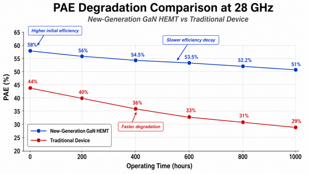
| [R] RF-Perf | PAE @ 28GHz * | ~25% – 35% | > 45% – 50% |
| [R] RF-Perf | Buffer Layer / Trapping Effects | Current collapse / Electrons escape 2DEG | Neutralized (Carbon/Iron-doped buffer) |
| [P] Packaging | Parasitic Inductance * | > 150 pH (Standard Wirebond/Legacy) | < 30 pH (Advanced Interface/Low-Parasitic) |
| [P] Packaging | Dielectric Passivation | Sub-optimal surface states | Optimized SiNx (Silicon Nitride) |
T: Thermal impedance optimization (Thermal)
In any high-frequency amplifier design, efficient thermal management directly determines the final electrical output performance. The new generation of die uses local substrate thinning technology and is combined with sintered silver and other high-conductivity thermal curing materials. This approach reduces the junction-to-case thermal resistance (Rth_JC) by up to 40% compared to using conventional gold tin (AuSn) soldering on thick substrates. Therefore, when selecting the type, the purchaser cannot only look at the data under ideal DC conditions, but must stare at the Rth_JC performance under the actual duty cycle.
R: RF Performance and Power Added Efficiency (RF-Performance)
Modern GaN HEMT devices can still maintain more than 50% PAE in Ka band, while it is rare for old products to exceed 35%. The reason why the gap is so large is that the new gate module design shortens the gate length to 0.15 microns or even 0.10 microns under the premise of ensuring the structural strength. The reduction of the gate-drain parasitic capacitance (Cgd) successfully pushed the cut-off frequency (fT) and the maximum oscillation frequency (fMAX) to above 150 GHz.
P: Advanced packaging reduces parasitics (Packaging)
In high-end HEMT GaN applications, air cavity ceramic packaging is rapidly replacing traditional overmolding plastic packaging technology. Traditional plastic packaging not only has a large dielectric loss, but also easily penetrates water vapor after long-term use. The advanced air cavity design can precisely control the length of the internal bonding wire, thereby minimizing parasitic inductance and maximizing broadband impedance matching capabilities.
Real Test Data: 28 GHz Power Amplifier Stress Test
Laboratory data confirm the theoretical advantages of modern epitaxial improvement techniques. Our team of engineers tested traditional GaN-on-Si HEMT and a new generation GaN-on-SiC HEMT at 28 GHz for up to 1000 hours of high temperature operating life (HTOL) continuous wave testing.
The results show that the power of the new generation devices is reduced by less than 0.2 dB during the whole test cycle. In contrast to traditional devices, there was a severe attenuation of 1.5 dB in the first 300 hours, and the main culprit was the soaring gate leakage current (I _GSS). The new generation of devices cleverly adopts a special T-shaped gate structure, which weakens the peak electric field at the edge of the gate and directly “misfires” the hot electron degradation effect “. For buyers of telecommunications infrastructure, the bill is a bargain: it means a significant increase in mean time between failures (MTBF) and a significant reduction in outfield maintenance costs.
Expert Demining: Avoiding The Trap Of “The Specification Is Out Of Touch With Reality”
A common mistake RF engineers make is to blindly believe the gorgeous data in the specification based on the ideal radiator, thus miscalculating the thermal budget.
Pit avoidance 1: Ignore the coefficient of thermal expansion (CTE) mismatch in high-power arrays
When choosing a high-density substrate, engineers often forget to consider the CTE difference between the die and the PCB material. In the state of high-power continuous wave, the solder joints of old components will produce micro-cracks due to the cyclic stress of thermal expansion and contraction. Selection standards now mandate the use of copper molybdenum (CuMo) or similar material fins to match the expansion rate of SiC.
Pit Avoidance 2: Ignore Dynamic R_DS(on) in Specification
The specifications of traditional devices always flaunt static DC resistance. However, developers must be truer and ask for “dynamic on-resistance” data measured at the actual application switching frequency. Static testing is like a fig leaf, covering up the trap effects that are enough to bring down the power supply or RF amplifier in the field.
Pit Avoidance 3: No evaluation of gate leakage current as a function of temperature
The gate leakage current of early products would soar wildly with increasing temperature, causing the bias point to shift and completely destroying linearity. The procurement team must explicitly require the device to pass the reverse gate bias stability test at 150°C to ensure that the digital pre-distortion (DPD) algorithm in modern telecommunications equipment still works in a variety of harsh environments.
Frequently Asked Questions (FAQ)
Why does the dynamic R_DS(on) of conventional HEMT GaN devices rise?
This is caused by electron traps in the epitaxial surface and in the buffer layer. When the device switches at high voltages, electrons get stuck in these structural defects, blocking current flow through the 2DEG channel, resulting in instantaneous power loss.
How do next-generation GaN HEMT devices improve power-added efficiency (PAE)?
This is mainly by significantly reducing parasitic capacitance (especially Cgd) and replacing it with an optimized GaN-on-SiC substrate. This not only speeds up heat dissipation and prevents carrier mobility degradation due to overheating, but also allows for shorter gate lengths (as low as 0.15 microns), making it easy to handle millimeter-wave bands.
Why do high-frequency applications prefer GaN-on-SiC to GaN-on-Si?
Because the thermal conductivity of silicon carbide (SiC) can be up to three times that of silicon. In high-frequency scenarios with extreme power densities, SiC can quickly draw heat away from the transistor junction region, avoiding the thermal frequency reduction and linearity degradation problems that silicon-based devices cannot escape.
How can engineers solve the thermal mismatch problem in GaN HEMT packages?
The key is matching the coefficient of thermal expansion (CTE) between the die and the flange/PCB. The industry usually uses advanced flange materials (such as copper molybdenum alloy CuMo) and high-reliability solid crystal process (such as sintered silver) to absorb the mechanical stress generated during thermal cycling.
What are the consequences of gate leakage current in conventional GaN components?
Leakage current will cause the static bias point of the amplifier to shift. This offset not only destroys the linearity of the signal and increases phase noise, but also undermines the highly dependent digital predistortion (DPD) systems found in modern 5G base stations.
Can traditional GaN devices meet future 6G bandwidth requirements?
Absolutely not. Due to excessive parasitic parameters and limited heat dissipation, traditional devices simply cannot reach the required cut-off frequency (fT) and maximum oscillation frequency (fMAX). 6G requires components that still maintain high efficiency and high linearity in the D band (110 GHz and above), which is undoubtedly the absolute home of the new generation of node structures.