 Neditek
GaN HEMT Power Amplifier:Unlocking Peak Efficiency
What Drives Peak PAE in GaN HEMT power amplifier?
A GaN HEMT power amplifier achieves its peak efficiency—often exceeding 70% Power-Added Efficiency (PAE) in sub-6GHz spectrums—by leveraging high breakdown voltages and low parasitic capacitances. RF engineers deploy these devices to replace aging LDMOS infrastructure in high-power continuous wave (CW) and pulsed radar applications. Translating lab-grade datasheets into field-ready base stations presents a specific set of challenges. Hardware teams routinely lose 10-15% of expected efficiency due to inadequate thermal dissipation routing, uncalibrated memory effects in wideband signals, and improper quiescent current drift management. Addressing these structural roadblocks separates standard designs from peak-performing RF front-ends.

The T.I.E. Efficiency Pyramid: Structuring RF Front-End Design
Engineering directors rely on the T.I.E. (Thermal, Impedance, Envelope) Efficiency Pyramid to standardize the integration of a gan power amplifier into complex telecom architectures. This framework forces design teams to resolve foundational physics before attempting software-level linearity corrections.
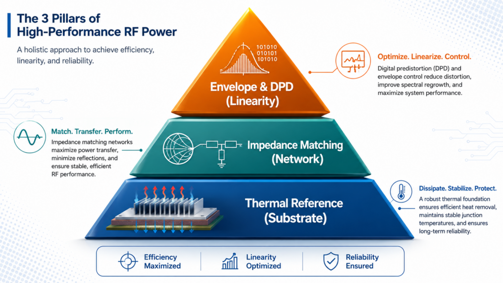
Thermal Baseline: Managing Junction Temperatures
Heat destroys RF performance long before it physically damages the semiconductor. A rising junction temperature (Tj) increases phonon scattering within the two-dimensional electron gas (2DEG) channel, degrading electron mobility and plummeting the PAE.
RF hardware arrays currently mandate GaN-on-SiC (Silicon Carbide) substrates for macro base stations. SiC provides a thermal conductivity of roughly 400 W/m·K, decisively outperforming standard GaN-on-Si variants. High-end radar systems are transitioning toward GaN-on-Diamond interfaces. This emerging substrate integration reduces the junction-to-case thermal resistance (RthJC) by an additional 30%, keeping continuous wave amplifiers well below the critical 200°C threshold and maintaining MTBF (Mean Time Between Failures) above 10⁶ hours.
Impedance Matching in Doherty Configurations
Achieving target bandwidth requires aggressive output impedance matching. The high output impedance of GaN devices relative to their immense power density simplifies matching networks compared to older GaAs equivalents. Engineers designing asymmetrical Doherty power amplifiers must precisely tune the offset lines. The peaking amplifier must present an open circuit to the main amplifier during back-off operation. Failure to optimize the output capacitance (Cout) absorption within the matching network causes immediate reflections, high VSWR (Voltage Standing Wave Ratio), and catastrophic efficiency drops at the frequency band edges.
Envelope Tracking and DPD Memory Compensation
Linearity and efficiency exist in direct opposition. Base station designers employ Envelope Tracking (ET) modulators to dynamically adjust the drain voltage in sync with the RF signal envelope. This prevents the amplifier from wasting DC power during signal troughs.
Applying Digital Pre-Distortion (DPD) to GaN HEMTs requires strict attention to charge trapping. Deep-level traps in the GaN crystalline structure create “memory effects,” where the amplifier’s current behavior depends on preceding signal pulses. Standard Volterra-series DPD algorithms fall short here. RF teams must implement memory-polynomial DPD models explicitly calibrated for wide-bandgap trapping dynamics to maintain ACLR (Adjacent Channel Leakage Ratio) below -50 dBc.
Real-World Failure Analysis: The Bias Sequencing Trap
Hardware prototyping phases frequently witness destroyed GaN devices due to minor sequencing errors. GaN HEMTs are inherently depletion-mode (normally-on) devices. Zero voltage on the gate means the drain-source channel is fully conductive.
The absolute primary rule of GaN PA integration is strict bias sequencing. Engineers must apply the negative pinch-off gate voltage (Vgs, typically around -5V) before applying any drain voltage (Vds, typically 28V to 48V). Applying Vds while the gate is at 0V causes a massive, instantaneous surge of short-circuit current (Idss) that vaporizes the device within microseconds.
Modern B2B equipment vendors mitigate this by integrating dedicated power management ICs (PMICs) that physically hardwire this sequencing, preventing junior engineers from bypassing the protocol during bench testing.
2026 Performance Benchmarks: Sub-6GHz and Radar
Procurement managers require verifiable metrics when selecting RF components. The following benchmark table reflects real-world testing data from top-tier 48V GaN HEMT platforms operating in Doherty configurations.
| Application Band | Operating Frequency | Output Power (W) | Target PAE (%) | Substrate Choice |
|---|---|---|---|---|
| 5G Sub-6GHz Macro | 3.3-3.8 GHz | 80W | 55-60% | GaN-on-SiC |
| X-Band Radar | 8-12 GHz | 100W Pulsed | 45-50% | GaN-on-SiC |
| SatCom Ka-Band | 26-30 GHz | 20W | 35-40% | GaN-on-SiC |
Evaluating these metrics shows a clear trajectory: increasing frequencies mandate tighter thermal budgets. B2B purchasing teams should prioritize vendors providing comprehensive load-pull data across the entire operating temperature range, not just optimal 25°C lab conditions.
FAQ
What is the difference between GaN HEMT and LDMOS power amplifiers?
GaN HEMTs offer significantly higher power density and operate at higher frequencies with greater efficiency than LDMOS. LDMOS technology hits physical efficiency limits above 3 GHz, whereas GaN easily scales into mmWave frequencies (up to 40 GHz and beyond) while maintaining high Power-Added Efficiency.
Why do GaN power amplifiers require negative gate voltage?
Most standard GaN HEMTs are depletion-mode devices, meaning the transistor channel is naturally open and conducting current. A negative gate voltage (typically between -2V and -5V) is mandatory to deplete the electrons in the channel and pinch off the current flow before high drain voltage is applied.
What is Power-Added Efficiency (PAE) in RF design?
PAE measures how effectively an amplifier converts DC input power into usable RF output power, factoring in the RF power already provided at the input. A higher PAE directly translates to lower heat generation, reduced cooling requirements, and lower operating costs for telecom operators.
How does GaN-on-SiC differ from GaN-on-Si?
GaN-on-SiC grows the gallium nitride layer on a silicon carbide substrate, offering superior thermal conductivity (managing high heat). GaN-on-Si uses a standard silicon substrate, which is cheaper to manufacture but suffers from inferior heat dissipation, restricting its use to lower-power commercial electronics rather than high-power base stations.
Can Digital Pre-Distortion (DPD) fix all GaN linearity issues?
No. While DPD excellently corrects standard amplitude and phase distortions, unmanaged thermal fluctuations and severe charge trapping cause unpredictable memory effects. Engineers must optimize the physical hardware matching and thermal routing before DPD software can effectively linearize the signal.