 Neditek
GaN HEMT Structure, Cross Section & Band Diagram Visualized
The core of how gallium nitride (GaN)HEMT works is that it can firmly “lock” the high-density two-dimensional electron gas (2DEG) at the AlGaN/GaN heterojunction. And you have to know that this is driven entirely by spontaneous polarization and piezoelectric polarization effects, and has nothing to do with traditional chemical doping.
Its physical structure directly determines the heat dissipation and mechanical limits of the device. Profile design (such as field plate and grid configuration) is responsible for the distribution of electric field. The energy band diagram is the “navigation map” that reveals the electron-confined quantum mechanical mechanism “. Although any device engineer can draw the physical laminated structure now, many people often roll over when doing TCAD simulation-unable to truly correspond the surface passivation state on the profile to the Fermi level pinning (Fermi level) in the energy band diagram. This is precisely the culprit of the model’s inability to accurately predict high-frequency dynamic on-resistance (Ron) degradation. Next, let’s get these 3 dimensions completely through and build a complete modeling framework.
P-E-C 3D Model: Decoding GaN Underlying Physics
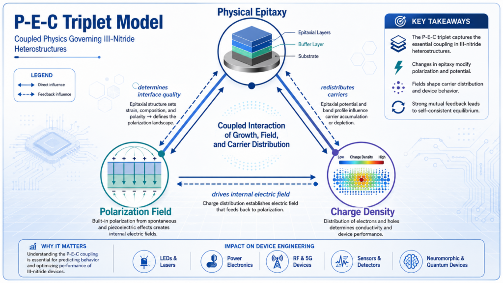
Many engineers are confused when it comes to linking physical manufacturing processes to microscopic quantum behavior. To this end, we have introduced a P-E-C (polarization-extension-charge) three-dimensional model specifically to fill this cognitive gap, linking macro variables to micro effects.
Polarization (Polarization, core driving force): The electric field inside the device is carried by spontaneous polarization and piezoelectric polarization. You don’t need to inject ions to get a charge like traditional silicon-based devices, what you have to do is to “pull” the lattice and create strain.
Epitaxy (Epitaxy, physical drawing board): What substrate to choose? How long and thick is the AlGaN barrier layer? These parameters directly determine the magnitude of the lattice strain.
Charge (Final Product): The polarization electric field and the surface donor state combine. How much 2DEG density there can be in the quantum well depends on the interaction between the two.
Get it? As long as you dare to move the physical size, the internal strain will change immediately, then the energy band will bend, and finally the concentration of 2DEG will be redefined.
From Macro To Micro: The Infrastructure Of GaN HEMTs
The macroscopic physical layout of GaN HEMT directly determines how much breakdown voltage it can carry and how fast heat it can dissipate. The choice of substrate and epitaxial growth process is the cornerstone of device reliability.
Substrate Material Determines Thermal Ceiling
Silicon carbide (SiC) thermal conductivity that is not to say, in high-power radio frequency (RF) work, it can quickly take away the heat in the channel; but the silicon (Si) substrate to win cheap, can significantly reduce the manufacturing cost. However, it should be noted that the lattice mismatch of the silicon substrate is extremely serious. In order to prevent the wafer from warping or even cracking of the epitaxial layer, a very complex stress relief transition layer must be made. Generally speaking, you have to be honest and practical SiC to be a RF base station, while Si is enough for consumer power electronics.
The key role of the buffer layer
In order to prevent substrate punch-through and leakage current, a carbon-doped GaN buffer layer is standard. Pure GaN is inherently n-type because of the presence of nitrogen vacancies. After the incorporation of carbon elements, it will introduce deep-level acceptor states, pulling the Fermi level away from the vicinity of the conduction band, thus making the buffer layer a semi-insulator. A fatal modeling mistake often arises here: many people think of the buffer layer as a purely rigid physical layer. In fact, under high voltage stress, these carbon traps will dynamically charge and discharge, directly change the internal electric field, and seriously slow down the switching speed of the device.
| Substrate Material | Lattice Mismatch to GaN | Thermal Conductivity | Primary Application Domain |
| Silicon Carbide (SiC) | Low (~3.5%)* | Superior (Extracts heat rapidly from the channel) | High-power RF operations, RF base stations |
| Silicon (Si) | Massive (Requires complex strain-relief transition layers to prevent wafer bowing/cracking) | Moderate / Lower than SiC | Consumer power electronics (Chosen to reduce manufacturing costs) |
| Sapphire* | High (~16%)* | Low (~35 W/m·K)* | Optoelectronics, LEDs, and standard RF devices* |
GaN HEMT Profile Structure: The Intersection Of Engineering And Physics
The cross-sectional design of the device is to turn the rough epitaxial layer of the stack into a good and obedient transistor. The geometric layout of the source, drain and gate, to put it bluntly, is to control the electric field distribution to prevent the device from being broken down in advance before it works.
AlGaN/GaN heterojunction and positioning of 2DEG
2DEG is not everywhere, it is precisely gathered at the junction of the thin AlGaN barrier layer and the thick GaN channel. The surface donor electrons will fall like a waterfall into the potential well formed by the heterojunction. The physical thickness of the AlGaN layer directly determines the distance between the gate metal and the 2DEG. If the AlGaN barrier layer is made thin under the gate, the transconductance can indeed be improved, but at the cost of sacrificing the maximum 2DEG surface density of the access regions.
Use Field Plates to Tame Electric Fields
The function of the source field plate is to reshape the electric field distribution and eliminate the electric field peak near the gate edge on the drain side. When a high voltage is applied to the drain, the equipotential lines will be frantically crowded in the corners of the gate, accelerating the electrons enough to cause impact ionization. The stepped field plate, on the other hand, can extend outward beyond the passivation layer and widen the depletion region outward on the physical level, thus dispersing the concentrated strong electric field into a number of small peaks with lower intensity. For any device with a rated voltage of more than 100V, this structure is used to save life and is essential.
Enhanced by p-GaN gate (E-Mode)
If a layer of p-type GaN is grown with extreme precision directly under the gate metal, the device can be forcibly turned Normally-off. You know, ordinary GaN HEMT is depleted (D-mode, normally on) because 2DEG is there under zero gate voltage. With the addition of this layer of p-GaN, it is like a local electronic “pump” (depletion zone), raising the conduction band energy at that specific location, and cutting off the 2DEG channel between the source and drain. Unless you put a forward voltage on the gate, it will never work.
See Through The Energy Band Diagram Of GaN HEMT

The band diagram not only allows you to see the electronic energy states deep in the device, but also to see the existence of 2DEG on a mathematical level. If you want to do a good job in device modeling, understanding that energy band bending is a hard indicator that is not negotiable.
Spontaneous Polarization and Piezoelectric Polarization Electric Field
The asymmetry of the lattice determines the slope of the polarization effect in the band diagram. The wurtzite crystal structure of GaN itself has no inversion symmetry, which makes the spontaneous polarization. Then you grow AlGaN on GaN, forcibly stretching the lattice of AlGaN, and then piezoelectric polarization is created. The superposition of these two polarization fields leads to a very sharp and linear tilt of the energy band the AlGaN barrier layer.
Formation of Triangular Quantum Wells
At the interface where AlGaN and GaN are in contact, the conduction band (Ec) falls extremely abruptly below the Fermi level (Ef). The positive polarity surface charge induced by polarization at the interface pulls the energy band down. Since the forbidden band width (3.4 eV) of GaN is narrower than that of AlGaN (assuming an aluminum composition of 25%, the band gap is about 4.0 eV), a conduction band shift (ΔEc) occurs here. Electrons are trapped in this sharp V-shaped sub-band potential well and can only move in a two-dimensional plane, which is the origin of 2DEG.
Fermi level pinning of the surface
In fact, the electrons that fill the 2DEG are in the surface state. The starting point of the band diagram is at the top of the device, where the Fermi level is firmly pinned because of the large number of donor-like surface traps. Electrons escape these high-energy surface states, either tunneling or drifting through the AlGaN barrier, and eventually falling into the low-energy quantum well. At this point, if we use silicon nitride (SiN) for surface passivation, we can neutralize those unstable traps, fix the surface potential, and prevent external environmental factors from “stealing” our 2DEG.
Expert Pit-Avoidance Guide: Dynamic On-Resistance And Buffer Layer Traps
Many engineers took the data of static direct current (DC) test to align the profile and energy band diagram model, and felt that it was perfect. As a result, they really put the finished physical devices into the dynamic power converter and ran and stopped eating directly. When our laboratory conducted a stress test on the 600V p-GaN HEMT, we found that there is a huge blind spot in the current modeling of “current collapse” (Current Collapse) or dynamic Ron degradation.
When the device switches 400V at a frequency of 100kHz, the electrons in the 2DEG will gain extremely high energy and even be deeply injected into the carbon-doped buffer layer. These electrons are then captured by the deep acceptor state. If you look at the dynamic band diagram at this time, you will find that these trapped negative charges move the conduction band of the GaN layer from the bottom to the top. This is the so-called “back-gate effect” (Back-gating), which will pinch off the 2DEG from below.
Standard TCAD simulations are often lazy, placing static flat band assumptions on the buffer layer. You have to manually define a set of transient trap emission distribution parameters in the device physical model. If the dynamic process of this deep level trap is not mapped out, the conduction band can drift up to 0.5eV under the turn-off bias. Reflected in physical hardware, dynamic Ron soared 30% or more without warning.
High Frequency Technical Q & A (FAQ)
Why can GaN HEMT form 2DEG without doping?
Because 2DEG is completely “forced” out by the polarized electric field. The physical strain between the AlGaN and GaN lattices creates a large internal electric field that directly sucks electrons from the surface donor states into the quantum well. Since there are no chemical impurities (doping ions) in the channel to act as a stumbling block, the electrons are not affected by the scattering of impurities, and the mobility is extremely high.
How does the p-GaN gate change the energy band diagram?
The addition of a layer of p-doped GaN above the AlGaN barrier can lift the entire energy band up at that location. At zero gate voltage, it can make the conduction band (Ec) directly higher than the Fermi level (Ef), thus depleting the local 2DEG. This operation changes the device from a normally-on (depletion mode) to a normally-off (enhancement mode) transistor in one fell swoop.
What is the AlN spacer layer (Spacer) used in the cross-sectional structure?
Usually between the AlGaN barrier layer and the GaN channel, the manufacturer will grow a very thin (usually only 1nm) aluminum nitride (AlN) spacer layer with extreme precision. Because AlN has a larger band gap than AlGaN, it creates a higher barrier in the band diagram. This can effectively prevent the electrons in 2DEG from “pouring back” into the AlGaN layer, greatly reducing alloy scattering and allowing electrons to run faster.
How does surface passivation affect 2DEG density?
Surface passivation (usually SiN silicon nitride) can stabilize the donor state of the surface. If there is no passivation layer, the surface potential will be high and low due to the change of the trapped charge, resulting in the band slope of the AlGaN layer to follow, thus depleting the 2DEG. The passivation process can “nail” the surface Fermi level in a fixed energy state, ensuring that the surface can stably transport the maximum amount of electrons to the channel.
Why does high-voltage GaN HEMT have to add field plates?
The field plate is to alleviate the electric field crowding problem near the drain side gate edge. In cross-section, the field plate is like a “protective umbrella” for the source or gate metal to extend out across the passivation layer “. It forces the depletion zone to expand in the horizontal direction. If there is no field plate, the peak electric field will exceed the critical breakdown threshold of GaN material in minutes, and the high-voltage device will be scrapped on the spot.
Why does the conduction band in the AlGaN barrier layer bend?
Because there is a very strong polarized electric field inside the AlGaN layer, this leads to a huge electrostatic potential difference between the surface and the heterojunction. According to the Poisson equation (Poisson’s equation), a constant electric field necessarily corresponds to a linear change in the electrostatic potential. If you map this onto the band diagram, you can visually see that the conduction and valence bands in the AlGaN region exhibit extremely steep, straight slopes.