
Search the whole station
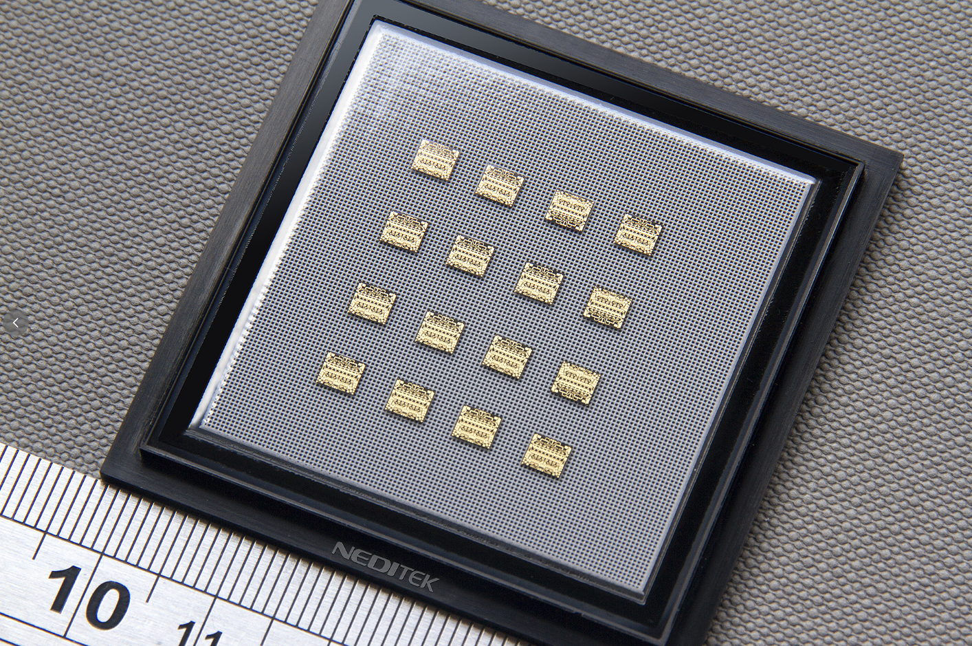
NEDITEK’s GaN power amplifiers deliver exceptional performance for high-frequency, high-power communications, thanks to their ultra-high power density enabled by GaN-on-SiC technology and a drain efficiency of up to 70%. NEDITEK is an IDM company with proprietary epitaxial growth capabilities and end-to-end production capacity for 4 and 6 inch wafers. By eliminating the middleman, we offer you more competitive factory-direct pricing and a more stable, mass-production supply.

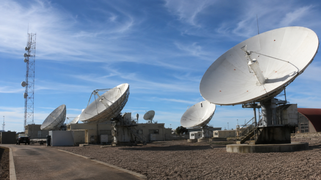
GaN power amplifiers are primarily used in 5G base station construction, wireless equipment, and satellite communication terminals.

the use of silicon carbide substrate high thermal conductivity, so that the device at the same power under the junction temperature reduced by more than 20 degrees, significantly improve the system stability and service life of high power operation.
achieve more than 50% efficiency under specific signals, reduce the heat dissipation pressure and power cost of the base station, and save about 30% energy for the system compared with traditional GaAs or Silicon devices.
A single chip can cover octave or even wider frequency range, reducing the number of amplifiers required in the system, making the RF front-end circuit layout more compact, and increasing the integration level by 40%.
the adjacent channel power ratio is better than negative 25 dB at rated output, ensuring that the signal is not distorted in a multi-carrier environment, effectively reducing the complexity of the development of digital pre-distortion algorithms.
using high temperature resistant metal ceramic packaging technology, the volume is only one tenth of the same power vacuum tube device, greatly reducing the occupied area of the RF front-end module in a narrow space.
Through more than 1 million hours of mean time between failures, it ensures continuous operation in outdoor extreme weather or harsh industrial environments, and reduces maintenance and replacement costs.
| Parameter Items | Technical Specifications Details |
| Product core keywords | GaN power amplifier |
| Coverage band | Includes P-band, L-band, S-band, C-band, X-band, and Ku-band |
| Typical saturation power | up to 58.5 dBm |
| Drain efficiency | Typical values are 54% to 70%. |
| Small signal gain | 22 to 25 dB |
| Adjacent channel power ratio | Better than -25 dB |
| Chip process node | 0.15 ~ 0.5 um |
| Operating ambient temperature | -55 +150 ℃ |
| Encapsulation type | Hermetic metal-ceramic encapsulation or flange mounting |
NEDITEK use leading GaN epitaxial technology, which has greater power tolerance and thermal management capabilities than traditional silicon-based gallium nitride devices. We have a deep accumulation in broadband matching technology, and a single-stage amplifier can meet the requirements of multi-band compatibility, reducing the difficulty of debugging peripheral matching circuits.

by optimizing the chip back metal process, the NEDITEK solves the technical pain point that the traditional high-power amplifier is prone to power drop due to excessive temperature rise when it is arranged in high density.
For the research and development of communication equipment, we have solved the problem that high linearity and high efficiency cannot be balanced, so that the system can meet the protocol standards while maintaining very low standby energy consumption.
As a factory with its own production line, NEDITEK solves the problem of unstable delivery and inability to provide in-depth customized services caused by over-reliance on imports of high-end RF devices.
For the design requirements of 5G macro and micro stations, provide high-efficiency, high-gain core power components to help reduce the overall network construction and operating costs.

Serves the construction group of low-orbit satellite terminals and ground stations, and solves the demanding demand for high-power output and high-reliability RF front-end in long-distance signal transmission.
for industrial heating, plasma excitation and medical microwave equipment, to provide continuous wave power output extremely stable power tube, instead of inefficient and large traditional magnetron.

Be sure to evenly apply high thermal conductivity silicone grease between the base and the radiator and apply standard torque for fastening to ensure that the working heat is discharged in time.

When starting, the negative bias power supply must be turned on first, and then the positive drain voltage must be turned on. the turn-off sequence is opposite. it is strictly prohibited to power on without negative pressure.

The input signal is strictly prohibited from exceeding the maximum safety value specified in the manual. It is recommended to configure a limiting protection device at the input end to prevent instantaneous overload from damaging the chip.

The output end should be connected with a low VSWR load, and the tightness of the connector should be confirmed before high-power debugging to avoid damage to the device due to impedance mismatch reflection.

Welcome to our Frequently Asked Questions page. We have compiled answers to common questions you may have, hoping to provide you with clear and quick solutions. If you cannot find the information you need here, please feel free to contact our customer support team.
NEDITEK’s GaN power amplifiers deliver exceptional performance for high-frequency, high-power communications, thanks to their ultra-high power density enabled by GaN-on-SiC technology and a drain efficiency of up to 70%. NEDITEK is an IDM company with proprietary epitaxial growth capabilities and end-to-end production capacity for 4 and 6 inch wafers. By eliminating the middleman, we offer you more competitive factory-direct pricing and a more stable, mass-production supply.
0.75 to 40 GHz
Frequency range
10 to 600 watts
Saturation output power
20 to 48 volts
Operating voltage

the use of silicon carbide substrate high thermal conductivity, so that the device at the same power under the junction temperature reduced by more than 20 degrees, significantly improve the system stability and service life of high power operation.
achieve more than 50% efficiency under specific signals, reduce the heat dissipation pressure and power cost of the base station, and save about 30% energy for the system compared with traditional GaAs or Silicon devices.
A single chip can cover octave or even wider frequency range, reducing the number of amplifiers required in the system, making the RF front-end circuit layout more compact, and increasing the integration level by 40%.
the adjacent channel power ratio is better than negative 25 dB at rated output, ensuring that the signal is not distorted in a multi-carrier environment, effectively reducing the complexity of the development of digital pre-distortion algorithms.
using high temperature resistant metal ceramic packaging technology, the volume is only one tenth of the same power vacuum tube device, greatly reducing the occupied area of the RF front-end module in a narrow space.
Through more than 1 million hours of mean time between failures, it ensures continuous operation in outdoor extreme weather or harsh industrial environments, and reduces maintenance and replacement costs.
| Parameter Items | Technical Specifications Details |
| Product core keywords | GaN power amplifier |
| Coverage band | Includes P-band, L-band, S-band, C-band, X-band, and Ku-band |
| Typical saturation power | up to 58.5 dBm |
| Drain efficiency | Typical values are 54% to 70%. |
| Small signal gain | 22 to 25 dB |
| Adjacent channel power ratio | Better than -25 dB |
| Chip process node | 0.15 ~ 0.5 um |
| Operating ambient temperature | -55 +150 ℃ |
| Encapsulation type | Hermetic metal-ceramic encapsulation or flange mounting |
by optimizing the chip back metal process, the NEDITEK solves the technical pain point that the traditional high-power amplifier is prone to power drop due to excessive temperature rise when it is arranged in high density.
For the research and development of communication equipment, we have solved the problem that high linearity and high efficiency cannot be balanced, so that the system can meet the protocol standards while maintaining very low standby energy consumption.
As a factory with its own production line, NEDITEK solves the problem of unstable delivery and inability to provide in-depth customized services caused by over-reliance on imports of high-end RF devices.
For the design requirements of 5G macro and micro stations, provide high-efficiency, high-gain core power components to help reduce the overall network construction and operating costs.
Serves the construction group of low-orbit satellite terminals and ground stations, and solves the demanding demand for high-power output and high-reliability RF front-end in long-distance signal transmission.
for industrial heating, plasma excitation and medical microwave equipment, to provide continuous wave power output extremely stable power tube, instead of inefficient and large traditional magnetron.
Be sure to evenly apply high thermal conductivity silicone grease between the base and the radiator and apply standard torque for fastening to ensure that the working heat is discharged in time.
When starting, the negative bias power supply must be turned on first, and then the positive drain voltage must be turned on. the turn-off sequence is opposite. it is strictly prohibited to power on without negative pressure.
The input signal is strictly prohibited from exceeding the maximum safety value specified in the manual. It is recommended to configure a limiting protection device at the input end to prevent instantaneous overload from damaging the chip.
The output end should be connected with a low VSWR load, and the tightness of the connector should be confirmed before high-power debugging to avoid damage to the device due to impedance mismatch reflection.
Please fill in the arithmetic result.
The calculation is incorrect, please fill it in again.
 Optimized by Seraphinite Accelerator