 Neditek
GaN RF Power Amplifier Chips
High Power RF Amplifier
Product Family: NDNC Series
NEDITEK's High Power RF Amplifier portfolio covers GaN power amplifier chips for RF transmit chains, with part-number options spanning different frequency bands, saturated output power, gain, PAE, bias voltage, VSWR, operating mode, and die dimensions. Request a part-number review to align the amplifier with your signal type, output target, thermal design, and package or integration level.
- Frequency Coverage0.3–43 GHz In Listed NDNC Entries
- PSAT26–49.6 dBm In Listed NDNC Entries
- PAE10–63% Where Reported
- Primary ApplicationRF Transmit Chains
- Supply PositionPart-Number Selection
- CustomizationTechnical Review Available
Family-level ranges are screening references; confirm the selected part number, test conditions, package and cooling path before purchase.
RF SELECTION & ACCEPTANCE
RF Selection And Acceptance Checklist
For an unspecified NDNC family record, the fastest route to a usable quote is to define the waveform, power reference, frequency, integration level and evidence needed for acceptance before choosing a part number.
Frequency And Waveform
State the target band, instantaneous bandwidth, CW or pulse operation, pulse width, repetition rate and duty cycle. A high-power label is not a universal watt threshold.
Power, Efficiency And Thermal
Record the required average and peak output, PSAT or compression target, gain, PAE, bias, thermal reference and cooling path. Do not combine best-case values from different test conditions.
Integration And Acceptance
Confirm bare die, transistor, MMIC or module form; RF ports and matching; load VSWR; bias sequence; models; fixture; calibration reference plane; and the test report fields before release approval.
COMPLETE SPECIFICATIONS
The Exact Data Buyers Need Before Ordering.
Family-level screening values are shown below. Confirm the selected NDNC part number and its approved test conditions before layout or purchase.
| Product Name | High Power RF Amplifier — NDNC Series |
|---|---|
| Model / Part Number | NDNC Series (Family-Level Selection Record) |
| Product Category | GaN RF Power Amplifier Chips |
| Frequency Coverage | 0.3–43 GHz Across Listed NDNC Entries |
| Representative Dimensions | Part-number dependent; listed examples include 3.7 × 5.5 × 0.08 mm and 4.0 × 6.0 × 0.08 mm |
| Material / Composition | GaN RF Semiconductor Technology |
| Connection / Interface | RF input/output and DC bias interfaces are part-number and package dependent; confirm from the approved data sheet |
| Documentation Basis | Part-number data sheet and stated test conditions |
| Marking / Traceability | Confirm batch / wafer traceability with the quotation |
| Packaging Unit | Bare die or package form varies by selected part number; confirm delivery form before order |
APPLICATIONS & EQUIPMENT
Where This Family Is Normally Evaluated.
Application fit depends on the waveform, reference plane, frequency, power level, linearity, thermal boundary and integration level recorded for the selected part.
Radar And Electronic Warfare
RF GaN power amplifiers can fit transmitter paths where pulse peak power, pulse width, duty cycle, phase stability and load mismatch are part of the selection record. Confirm the target band and pulse conditions against the selected part number.
Base Station And Wireless Communications
For modulated communication chains, screen the waveform band, instantaneous bandwidth, average power, efficiency, linearity, ACLR/EVM and thermal behavior together; CW Psat alone is not a substitute.
Satellite, Test And Microwave Systems
Satellite links and broadband test chains require a defined frequency reference, output reference plane, package or integration level, stability, protection and cooling plan before device or module selection.
MATERIALS & MANUFACTURING
How The Supplied Family Is Developed And Finished.
The local product record identifies GaN RF power amplifier chips, while the company capability record describes chip design, wafer processing, packaging and testing. The exact stack, metallization, package finish and process revision remain part-number specific.
Material / Grade
GaN RF Semiconductor Technology
Manufacturing Process
Chip Design, Wafer Processing, Packaging And Testing Are Described In The Company Capability Record
Surface / Finishing
Package Finish Or Die Metallization Is Part-Number Dependent; Confirm Before Layout
PERFORMANCE & WORKING CONDITIONS
Compare Family-Level Performance Before Selecting A Part Number.
The ranges below summarize the listed NDNC table. They are screening references, not a single-model guarantee; use the approved part-number data sheet and test conditions for release decisions.
CUSTOMIZATION
Align The Technical Review To The New RF Design.
Company service materials describe design support and customization. The items below define a review scope; any deliverable, tooling or commercial commitment requires quotation approval.
- Frequency And Band Review
Confirm a part-number option against the target band and instantaneous bandwidth. - Output Power And Operating Mode
Separate CW, PL/CW, PL and Pulse requirements before quotation. - Bias And Interface Review
Confirm VD, IDQ, RF ports, matching and bias sequencing for the selected record.
- Package Or Integration Level
Screen bare die, transistor, MMIC or module form. - Thermal And Mounting Review
Align package, thermal reference, cooling path and load-mismatch protection. - Documentation And Test-Plan Alignment
Request the approved data sheet, models and test conditions needed for acceptance.
FACTORY & MANUFACTURER
Know Who Makes And Supports This Family.
The task identifies the manufacturer and supplies a factory image; the local company record supplies the RF capability summary. Confirm the legal entity and selected delivery form on the quotation.
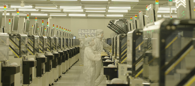
Ntesy Technology Company Limited (NEDITEK)
NEDITEK's company record describes RF product development across chip design, wafer processing, packaging, testing, quality control, module integration and system solutions. The RF portfolio includes Si, GaAs and GaN power amplifiers, transistors, control chips and RF modules; exact manufacturing entity and product delivery form should be confirmed in the quotation.
- 524 Zhongshan East Road, Nanjing, Jiangsu Province, China
- Chip design, wafer processing, packaging and testing capability
- RF power amplifiers, transistors, control chips and modules
- Design support and customization subject to technical review
REQUEST A TECHNICAL QUOTE
Tell Us The Equipment, Condition And Quantity.
- Phone: +86 25 8685 8581
- Email: sales@neditek.com
- WhatsApp: +86 25 8685 8581
- 524 Zhongshan East Road, Nanjing, Jiangsu Province, China