
Iv Characteristics Mosfet
The I-V characteristic curve of MOSFET essentially describes the “game” relationship between terminal voltage and drain current, which is not only the core of semiconductor physics, but also the foundation of digital switch and analog amplifier circuit design. If you want to really understand MOSFET, you must crack these 3 working areas: the cut-off area, the linear area and the saturation area.
In the cut-off region, when the gate-source voltage (Vgs) is less than the threshold voltage (Vth), the device is basically in a dormant state, and the effective value of the drain current is almost zero. Once Vgs crosses the threshold of Vth, the MOSFET enters the linear region (where Vds < Vgs – Vth) and behaves like a voltage-controlled resistor, with Id growing proportionally as the drain-to-source voltage (Vds) increases. When Vds further increases to the “pinch-off” point (I. e. Vds ≥ Vgs – Vth), the device cuts into the saturation region. At this time, the inversion layer at the drain end disappears, and Id is no longer at the mercy of Vds, but dominated by the square term of (Vgs – Vth). Understanding these curves—especially the output characteristics (Id vs. Vds) and transfer characteristics (Id vs. Vgs)—is the basic skill for calculating transconductance (gm), dealing with channel length modulation effects and ensuring stable performance of complex circuits.
Basic Logic For MOSFET Operation

MOSFET is actually a 4-side device. by applying voltage (Vgs) to the gate, we can control the current between drain and source like a faucet.
This electrical behavior is mainly represented by two types of key curves:
- Output characteristic curve: under different Vgs steps, plot the trajectory of Id changing with Vds.
- Transfer characteristic curve: Under fixed Vds, observe how Id fluctuates with the change of Vgs.
Detailed Explanation Of Three Working Areas
The core of understanding the I-V curve is to disassemble the “temper” of the MOSFET under different bias conditions.
1. Off State
The determination condition for this area is simple: Vgs < Vth.
Even if you apply a higher voltage (Vds) to the drain, the channel between the source and drain cannot be formed. At this point the device is like a circuit breaker. In industrial applications and smart grids, which have extremely high requirements for high reliability, whether the leakage current in the cut-off area is well controlled is directly related to the energy consumption efficiency of the entire system.
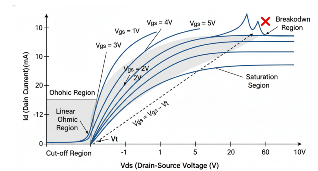
- Drain current (Id): ≈ 0 A
2. Linear/Ohmic Region
When Vgs > Vth and Vds < (Vgs – Vth), the MOSFET enters the linear region. The induced channel is then uniform and the device behaves like a resistor controlled by the gate voltage.
- Property: Id increases linearly with increasing Vds.
- Simplified formula: Id = k * [2 (Vgs – Vth) Vds – Vds²]
- Practical application: In automotive electronics and household appliances, when the MOSFET is used as a closed switch, it mainly works in this area.
3. Saturation Area
As Vds continues to increase and satisfies Vds ≥ (Vgs – Vth), the channel thickness near the drain terminal decreases to zero, which is a so-called “pinch-off” phenomenon. After that, even if you increase Vds, Id will not increase significantly.
- Characteristics: Id tends to be constant and is only controlled by Vgs.
- Square law formula: Id = (1/2) * k * (Vgs – Vth)²
- Importance: This is the golden area of signal amplification. When dealing with wireless communication and microdisplay technology solutions, NEDITEK technical experts will focus on the linearity and stability of these 1 areas.
In-depth Analysis
Output Properties
These curves show how the MOSFET slides from “resistive” mode to “constant current source” mode. By observing the 1 set of curves at different Vgs, engineers can quickly lock the output resistance (ro).
This chart reflects the “gain” capability of the device. It intuitively tells us the efficiency of the gate voltage control current. From this we can derive the transconductance (gm), which is the ratio of the change in drain current to the change in gate voltage:
- gm = ΔId / ΔVgs
High transconductance means that the device is more sensitive and efficient, which is essential for high-frequency response in rail transit signal systems and space exploration missions.
Non-Ideal Effects: Channel Length Modulation
In practical engineering, the drain current in the saturation region is not a straight line at the level of the 1 root. Due to the channel length modulation effect, the effective channel length actually shrinks as Vds increases. We usually use the parameter λ (Lambda) to correct.
- Modified saturation current formula: Id = (1/2) * k * (Vgs – Vth)² * (1 + λ Vds)
For precision engineering that meets NEDITEK stringent standards, analog circuits must be designed with λ in mind, otherwise gain errors can be a headache.
Why Are I-V Characteristics So Important In Modern Industry?

Mastering the I-V characteristics of MOSFETs is by no means just to cope with exams. It directly determines the performance ceiling in the following areas:
- Wireless communications: Optimizing power amplifiers in 5G/6G infrastructure.
- Automobiles and New Energy: Ensure high efficiency of power conversion in electric vehicles (EV).
- Mobile terminal: by using the cut-off area to completely eliminate the “dark current”, so as to extract the last 1 drops of battery life.
- Aerospace and Exploration: Stable operation of the circuit is maintained despite Vth drift due to extreme environments.
