Search the whole station
| Part Number | Operating Voltage VCE (V) | Operating Current IC (mA) Rec. | Operating Current IC (mA) Max | Forward Current Gain hFE (Ω) Min | Forward Current Gain hFE (Ω) Max | Frequency Cutoff fT (GHz) f=500MHz Min | Frequency Cutoff fT (GHz) f=500MHz Typ | Insertion Power Gain |S21E|2 (dB) f=2GHz Typ | Noise Figure NF (dB) f=2GHz Max | Package |
| NDGD250001 | 8 | 20 | 65 | 50 | 200 | 6.5 | 8 | 9 | 2.5 | Bare Die |
| NDGD250002 | 8 | 20 | 65 | 50 | 200 | 6.5 | 8 | 9 | 2.5 | ST-29 |
| NDGD250006 | 8 | 7 | 20 | 50 | 200 | 5 | 8 | 6.5 | 2.5 | Bare Die |
| NDGD250007 | 8 | 7 | 20 | 50 | 200 | 5 | 8 | 6.5 | 2.5 | ST-29 |
| NDGD250008 | 8 | 15 | 40 | 50 | 200 | 5 | 8 | 6.5 | 2.5 | Bare Die |
| NDGD250009 | 8 | 15 | 40 | 50 | 200 | 5 | 8 | 6.5 | 2.5 | ST-29 |
| NDGD250010 | 8 | 25 | 80 | 50 | 200 | 5 | 8 | 6.5 | 2.5 | Bare Die |
| NDGD250011 | 8 | 25 | 80 | 50 | 200 | 5 | 8 | 6.5 | 2.5 | ST-29 |
| NDGD250012 | 8 | 70 | 160 | 50 | 200 | 5 | 8 | 6.5 | 2.5 | Bare Die |
| NDGD250003 | 8 | 70 | 160 | 50 | 200 | 5 | 8 | 6.5 | 2.5 | ST-29 |
| NDGD250013 | 3 | 5 | 10 | 50 | 200 | 10 | 11 | 12.5 | 2 | Bare Die |
| NDGD250004 | 3 | 5 | 10 | 50 | 200 | 10 | 11 | 12.5 | 2 | ST-29 |
| NDGD250014 | 3 | 15 | 35 | 50 | 200 | 10 | 11 | 12.5 | 2 | Bare Die |
| NDGD250005 | 3 | 15 | 35 | 50 | 200 | 10 | 11 | 12.5 | 2 | ST-29 |
Technological Differences

IDM
Full IDM capability covering epitaxy, wafer, packaging,
ensuring stable supply and consistent performance.

Integration
Proprietary Si/GaAs/GaN technologies, with products spanning DC to
100 GHz for high-power, high-efficiency applications.

More Reliable
Strong customization and system-level design, providing
one-stop solutions from bare die to SIP & microsystems.
Technological Differences
IDM
Full IDM capability covering epitaxy, wafer, packaging,
ensuring stable supply and consistent performance.
Integration
Proprietary Si/GaAs/GaN technologies, with products spanning DC to
100 GHz for high-power, high-efficiency applications.
More Reliable
Strong customization and system-level design, providing
one-stop solutions from bare die to SIP & microsystems.
Audience Profile
RF & mm Wave Design Engineers
Pursue ultra-low parasitics & signal integrity for 100 GHz+ applications.
Test Instrument Architects
Need ultra-stable, low-noise RF components for precision test & measurement systems.
Power Electronics Designers
Seek high-efficiency SiC/Si devices for EV & industrial power systems.
Optoelectronics R&D Teams
Need high-performance OLED microdisplays & photodetectors for AR/VR & night vision.
Audience Profile
RF & mm Wave Design Engineers
Pursue ultra-low parasitics & signal integrity for 100 GHz+ applications.
Test Instrument Architects
Need ultra-stable, low-noise RF components for precision test & measurement systems.
Power Electronics Designers
Seek high-efficiency SiC/Si devices for EV & industrial power systems.
Optoelectronics R&D Teams
Need high-performance OLED microdisplays & photodetectors for AR/VR & night vision.
Handling & Operating Guidelines
Storage & Environment
Store in N2 cabinets/Gel-Pak; operate in Class 10,000 cleanroom.
ESD Precautions
ESD sensitive; grounded wrist straps and workstations required.
Handling & Pick-up
No metal tweezers on chip body; use vacuum tools or ESD-safe plastic tweezers on leads only.
Assembly & Bonding
Thermocompression: Stage 150℃ / Tool 250℃; precise force control.
Handling & Operating Guidelines
Storage & Environment
Store in N2 cabinets/Gel-Pak; operate in Class 10,000 cleanroom.
ESD Precautions
ESD sensitive; grounded wrist straps and workstations required.
Handling & Pick-up
No metal tweezers on chip body; use vacuum tools or ESD-safe plastic tweezers on leads only.
Assembly & Bonding
Thermocompression: Stage 150℃ / Tool 250℃; precise force control.
Construction & Compliance
Parts & Materials /
Composition
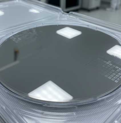
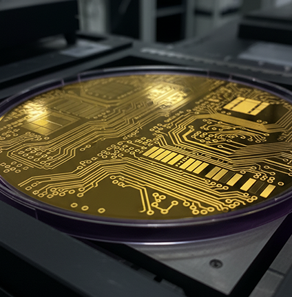
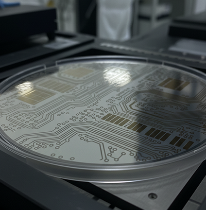
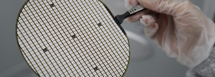
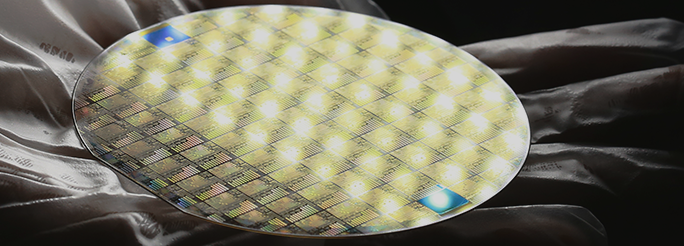
Built with Precision, Engineered for Performance.” NEDITEK’s GaAs/GaN RF/mmWave chips feature optimized material architectures: GaAs devices deliver stable 100 GHz+ performance via gold metallization, semi-insulating GaAs substrates, and silicon nitride/glass passivation;
Substrate
High-purity SiC / GaAs / Silicon
Metallization
Multi-layer gold
Passivation
Silicon Nitride
Expert Support & Service Assurance
Pre-sales: Accelerating Your Design
Solution Customization & Selection Guidance —— Senior RF engineers provide tailored component matching for your frequency, power, and performance requirements.
Simulation Model Support —— Comprehensive S-parameters, test report, and EVB to shorten your design cycle.
Rapid Sampling Service —— Fast sample delivery for standard and custom products to support early-stage R&D.
After-sales: Quality & Supply Assurance
Assembly Process Consulting —— Detailed guidance for thermocompression bonding and assembly processes.
Failure Analysis (FA) Services —— Professional root-cause diagnosis and corrective actions for assembly/test anomalies.
Supply Chain Continuity —— Long-term PCN/EOL management and buffer stocking for stable, uninterrupted supply.
Expert Support & Service Assurance
Pre-sales: Accelerating Your Design
Solution Customization & Selection Guidance —— Senior RF engineers provide tailored component matching for your frequency, power, and performance requirements.
Simulation Model Support —— Comprehensive S-parameters, test report, and EVB to shorten your design cycle.
Rapid Sampling Service —— Fast sample delivery for standard and custom products to support early-stage R&D.
After-sales: Quality & Supply Assurance
Assembly Process Consulting —— Detailed guidance for thermocompression bonding and assembly processes.
Failure Analysis (FA) Services —— Professional root-cause diagnosis and corrective actions for assembly/test anomalies.
Supply Chain Continuity —— Long-term PCN/EOL management and buffer stocking for stable, uninterrupted supply.
NEDITEK employs a unified, high-standard quality management system (QMS) tailored to semiconductor manufacturing, covering silicon-based ICs, GaAs/GaN RF devices, power electronics (SiC/Silicon), and OLED microdisplays. We implement strict process control and traceability systems across the entire IDM chain—from epitaxy and wafer fabrication to metallization, packaging, and final testing. By standardizing core processes and leveraging automated inspection platforms, we guarantee consistent performance, reliability, and dimensional accuracy across all product categories, meeting the stringent requirements and consumer applications.
All NEDITEK products, including power semiconductors (SiC/GaN MOSFETs/SBDs) and multi-functional silicon ICs, comply with widely recognized international industry standards and high-grade quality requirements for demanding applications. We perform comprehensive reliability validation customized for each product category: power devices are tested under high-temperature reverse bias (HTRB), high-humidity conditions, and dynamic stress to ensure high efficiency and long-term operational stability; silicon-based multi-functional chips are verified for wide environmental adaptability and consistent signal performance. Adherence to ISO, IATF, and industrial-grade quality standards ensures reliable performance in harsh industrial, automotive, and high-reliability commercial environments.
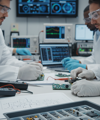
NEDITEK maintains exceptional manufacturing precision and high, stable yields for high-value products including RF devices, power semiconductors, silicon-based multi-functional ICs and OLED microdisplays. We operate in strictly controlled cleanroom environments, implement real-time statistical process control, conduct full-process in-line testing and full-lifecycle traceability, and apply AI-driven quality optimization to minimize variations, eliminate defects, and ensure consistent performance across every batch.
NEDITEK has built a comprehensive testing & FA laboratory covering all product lines. We provide full electrical parameter testing (including S-parameters, power characteristics, and display performance), environmental stress testing (temperature cycling, vibration, radiation), and advanced failure analysis (scanning electron microscopy, X-ray inspection, thermal analysis). Our professional engineering team delivers detailed FA reports and corrective action plans, helping customers quickly resolve design-in and manufacturing issues—accelerating R&D iteration and ensuring product robustness.
As a vertical IDM manufacturer, NEDITEK controls the entire supply chain from substrate procurement to final production, eliminating third-party dependency risks. We implement end-to-end traceability systems for every batch of wafers, components, and finished products, enabling full lifecycle tracking. For high-volume and long-cycle projects, we maintain buffer stock planning, PCN/EOL lifecycle management, and flexible production scheduling. This ensures uninterrupted supply, on-time delivery, and consistent quality across silicon, RF, power electronics, and microdisplay product lines.
NEDITEK leverages proprietary process integration technologies to optimize performance, size, and reliability. We adopt advanced packaging solutions (such as SIP and system-level integration) for multi-functional chips to reduce footprint while enhancing signal processing efficiency; for power devices, we optimize SiC wafer processes and thermal management designs to achieve high power density, low loss, and excellent heat dissipation. These optimizations ensure our power products meet the strict size, efficiency, and reliability requirements of compact industrial systems, automotive electronics, and other high quality platforms.
Manufacturing Excellence & Quality Assurance
Manufacturing Excellence & Quality Assurance
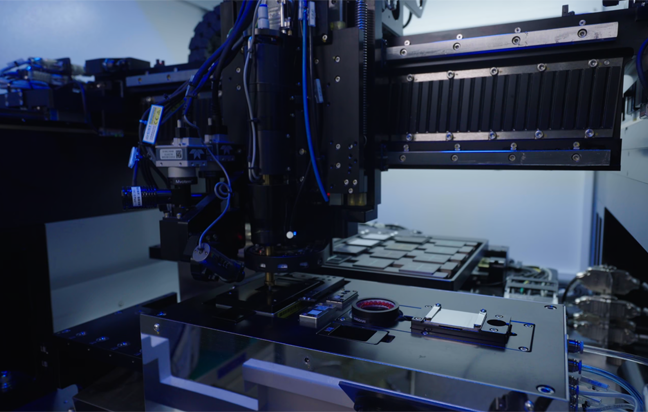
NEDITEK employs a unified, high-standard quality management system (QMS) tailored to semiconductor manufacturing, covering silicon-based ICs, GaAs/GaN RF devices, power electronics (SiC/Silicon), and OLED microdisplays. We implement strict process control and traceability systems across the entire IDM chain—from epitaxy and wafer fabrication to metallization, packaging, and final testing. By standardizing core processes and leveraging automated inspection platforms, we guarantee consistent performance, reliability, and dimensional accuracy across all product categories, meeting the stringent requirements and consumer applications.
All NEDITEK products, including power semiconductors (SiC/GaN MOSFETs/SBDs) and multi-functional silicon ICs, comply with widely recognized international industry standards and high-grade quality requirements for demanding applications. We perform comprehensive reliability validation customized for each product category: power devices are tested under high-temperature reverse bias (HTRB), high-humidity conditions, and dynamic stress to ensure high efficiency and long-term operational stability; silicon-based multi-functional chips are verified for wide environmental adaptability and consistent signal performance. Adherence to ISO, IATF, and industrial-grade quality standards ensures reliable performance in harsh industrial, automotive, and high-reliability commercial environments.
NEDITEK maintains exceptional manufacturing precision and high, stable yields for high-value products including RF devices, power semiconductors, silicon-based multi-functional ICs and OLED microdisplays. We operate in strictly controlled cleanroom environments, implement real-time statistical process control, conduct full-process in-line testing and full-lifecycle traceability, and apply AI-driven quality optimization to minimize variations, eliminate defects, and ensure consistent performance across every batch.
NEDITEK has built a comprehensive testing & FA laboratory covering all product lines. We provide full electrical parameter testing (including S-parameters, power characteristics, and display performance), environmental stress testing (temperature cycling, vibration, radiation), and advanced failure analysis (scanning electron microscopy, X-ray inspection, thermal analysis). Our professional engineering team delivers detailed FA reports and corrective action plans, helping customers quickly resolve design-in and manufacturing issues—accelerating R&D iteration and ensuring product robustness.
As a vertical IDM manufacturer, NEDITEK controls the entire supply chain from substrate procurement to final production, eliminating third-party dependency risks. We implement end-to-end traceability systems for every batch of wafers, components, and finished products, enabling full lifecycle tracking. For high-volume and long-cycle projects, we maintain buffer stock planning, PCN/EOL lifecycle management, and flexible production scheduling. This ensures uninterrupted supply, on-time delivery, and consistent quality across silicon, RF, power electronics, and microdisplay product lines.
NEDITEK leverages proprietary process integration technologies to optimize performance, size, and reliability. We adopt advanced packaging solutions (such as SIP and system-level integration) for multi-functional chips to reduce footprint while enhancing signal processing efficiency; for power devices, we optimize SiC wafer processes and thermal management designs to achieve high power density, low loss, and excellent heat dissipation. These optimizations ensure our power products meet the strict size, efficiency, and reliability requirements of compact industrial systems, automotive electronics, and other high quality platforms.
Start The Conversation
From standard to bespoke, we provide precise support. Let’s create value together.
Start The Conversation
From standard to bespoke, we provide precise support. Let’s create value together.
Please fill in the arithmetic result.
The calculation is incorrect, please fill it in again.
 Neditek