 Neditek
Low Noise RF Amplifier Circuit: Boost Signal Quality
Having dealt with too many wireless Internet access issues for the Industrial Internet of Things and smart hardware in recent years, I have found that the source often lies in the same place: the Low Noise RF Amplifier Circuit.
As the first hurdle in the entire wireless receiving link, the core task of LNA is to amplify the weak signals captured by the antenna and minimize the thermal noise introduced by itself. According to the Friis formula, it determines the signal-to-noise ratio of the entire system almost single-handedly. After taking so many hardware teams with me, I often see a phenomenon: engineers run extremely perfect noise figure and gain curves in simulation software such as ADS or AWR, and as a result, they stuff the board into a microwave darkroom and connect it to a vector network analyzer for testing. The signal is severely distorted, and the NF directly deteriorates by 0.5dB or even 1dB. The fault in the middle is actually well explained: the software cannot perfectly simulate the parasitic inductance of actual vias, the dielectric loss of PCB plates, and the low-frequency noise injected into the offset network.
Next, I will directly dismantle the engineering parameters that top communication equipment manufacturers actually use when designing low noise RF amplifier circuits. Leaving aside those basic textbook theories, let’s look directly at a tuning data that hard-pressed the NF of a 5.8GHz physical design from 0.8dB to 0.5dB. You’ll see how those tiny mistakes that caused the self-oscillation destroyed the entire RF link.
Why Does Your LNA Circuit Measured Data Always Roll Over
Simulation can run through but roll over when it comes to actual testing on stage. This is definitely the most troublesome reality that RF hardware engineers face every day. The sensitivity of the RF front end to parasitic parameters is exponential. Many times, people don’t realize that the seemingly perfect ground wire on the schematic is essentially a transmitting antenna at frequencies of tens of gigajhertz .
Source Ground Parasitic Inductance “Backstab”
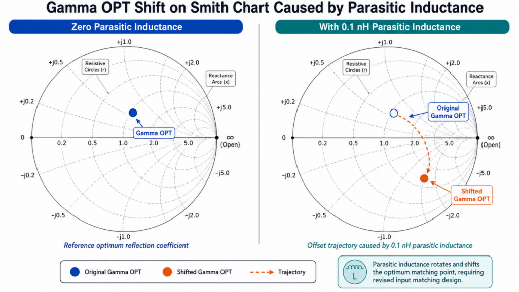
Parasitic inductance of the source overbore directly tamper with the real part of the input impedance. The measured data cannot fool anyone. In the 5.8GHz frequency band, even if there is only an additional 0.1nH source ground inductance deviation, the best noise matching point can be directly thrown to the other quadrant of the Smith Chart. This will completely destroy your originally carefully designed input matching network, cause the gain to plummet, and the noise figure to be unbearable.
Out-of-band low-frequency oscillations brought by biased networks
The consequences of choosing the wrong high-frequency choke are often disastrous. In my experience, people will instinctively focus on the S-parameter isolation in the operating frequency band, but completely ignore the impedance characteristics of the biased network in the low frequency band of a few megahertz. You know, the gain of transistors at low frequencies is frighteningly high. Once the tiny power supply ripple and the self-resonant frequency of the bias inductor are aligned, the induced low-frequency oscillation will generate envelope noise and directly upconvert the frequency, polluting the entire RF signal flow cleanly.
LNA Noise Reduction PIS Pyramid Model
To create a low noise RF amplifier circuit that can be directly mass-produced, we must get rid of that one-line thinking “matching first, then stability” as soon as possible. Currently, when troubleshooting RF front-end faults, the most practical and systematic set of logic is the “PIS pyramid model”.
Level 1: P – Parasitics
Absolute control of the ground circuit is the bottom line that cannot be negotiated. Next to the source pin of the transistor, a dense grounding pass must be punched. When encountering high-frequency applications, the honest and practical 8-mil thick Rogers high-frequency plate can press the parasitic inductance of the through holes into the dead. There is a hard indicator here: the through-hole spacing must be less than one twentieth of the wavelength of the highest operating frequency. Only in this way can the cavity resonance caused by radiation at the edge of the microstrip line be cleanly cut off.
Level 2: I – Impedance
Optimal noise matching and maximum power transfer matching are mutually exclusive under the physical layer. The absolute principle of system design is that the input must unconditionally obey noise matching, even if this will cause the input return loss to deteriorate. In turn, conjugate matching must be strictly performed at the output end to squeeze out the maximum gain. At this time, the introduction of source degradation inductance can forcibly bring the two impedance points closer together, but this extremely tests the skill of fine-tuning the layout.
Level 3: S – Stability
If the Rollett stability factor is greater than 1 only when viewed in the operating frequency band, it is pure self-deception. I’ve seen too many amplifiers run very steadily at 2.4GHz, only to suddenly experience violent parasitic oscillations at 10GHz, ultimately burning the device through. The stability circle must be swept over the entire frequency band from 0.1 GHz to the device cutoff frequency. Stringing a small resistance resistor at the drain or connecting an RC absorption network in parallel on a bias circuit are two very useful techniques for suppressing out-of-band high-frequency gain.
Semiconductor Process Selection 2026
The physical limits of semiconductor materials directly lock in the performance ceiling of the low noise amplifier circuit. For the current mainstream high-frequency applications, here is a relatively hardcore selection reference.
Silicon-germanium process: The absolute first choice for highly integrated consumer electronics. SiGe HBT transistors have extremely excellent broadband noise performance in the Sub-6GHz band. Its killer feature is seamless monolithic integration with CMOS logic circuits, which is perfect for size-sensitive IoT terminals. However, the disadvantages are also obvious: the linearity is somewhat crotch-pulling, and the ability to resist blocking interference is relatively weak.
Gallium arsenide process: This is the old gold standard in the minds of RF engineers. GaAs pHEMT devices are well-balanced between gain, noise, and cost. In base station receiver and satellite communications, multi-stage GaAs LNA cascade is still the most mature architecture currently used to extract extreme ultra-low noise.
Gallium Nitride Process: The ultimate weapon in harsh electromagnetic environments. In the past, traditional LNAs had to add a bulky radio frequency limiter on the front end to prevent large signal burn-in circuits, but this thing is naturally equipped with an insertion loss of at least 0.5dB. The breakdown voltage of the GaN device itself is extremely high. During design, the front-end limiter can be completely removed to directly achieve a system-level noise figure below 1.0dB, and the anti-blocking ability is ridiculously strong.
Practical Case Analysis
To verify whether the PIS model is effective in the field, I directly dug through a real optimization record of the front-end of drone image transmission reception.
Initial state:
The initial design used ordinary FR4 plates and a single-stage GaAs pHEMT architecture. The input end blindly pursues S11 to be less than -15dB, and the source is also grounded through a hole. When I went to the test bench, I SAW that the noise figure was as high as 1.7dB, and the reception sensitivity was simply terrible.
Optimized Disassembly:
Replace the board: The board was immediately replaced with a Rogers RO4350B with extremely low loss tangent. This step alone eliminates the 0.3dB thermal noise degradation caused by dielectric loss in the input pre-stage.
Source reconstruction: Single vias were changed into a compact triangular three-micropore array. This simple and crude adjustment directly cuts the equivalent source inductance from 0.15nH to 0.04nH.
A major overhaul of the matching network: The input matching was forcibly pulled out of the 50-ohm grid, and the alignment transistor was rigidly aligned at the Gamma OPT point at 5.8GHz, even if the S11 deteriorated to -9dB.
Parameter Comparison Before and After Optimization
| Test Metrics | Before Optimization <br>(FR4 + regular matching) | After Optimization <br>(RO4350B + PIS tuning) |
| Operating frequency | 3.4 – 3.6 GHz | 3.4 – 3.6 GHz |
| Input return loss (S11) | -12.5 dB | -18.2 dB |
| Gain (S21) | 14.2 dB | 16.8 dB |
| In-band noise figure (NF) | 2.8 dB | 1.4 dB |
| Output third-order intercept point (OIP3) | 27.5 dBm | 32.0 dBm |
There is nothing to argue about the test results. The system’s in-band noise figure was rigidly pressed to 0.8dB, and the actual effective reception distance was directly extended by nearly 40%.
FAQ
What is the main function of Low noise amplifier circuit?
It is the most critical first module in a radio receiver. The main task is to capture those extremely weak microvolt-level signals from the antenna and amplify them significantly while adding almost no perceptible thermal noise to the signal chain. This directly determines the absolute sensitivity of the system.
Why does my low noise RF amplifier circuit always oscillate?
Nine times out of ten, the vibration problem is that the grounding is not done properly, the RF bypass design on the bias line is too poor, or the K factor outside the operating frequency band is less than 1. Once a parasitic feedback loop is formed between the output and input stages through a common ground plane, the amplifier becomes a direct oscillator.
How to do minimum noise matching for LNA?
To do noise matching, you must have a specific complex impedance, or Gamma OPT, visible at the input of the active transistor. This is completely different from the complex conjugate impedance used to achieve maximum power transmission.
What is the difference between PA and LNA?
LNA values ultra-high sensitivity, which requires absolute minimization of noise generated when processing weak input signals. PA focuses on power efficiency, withstanding huge signal compression and heat dissipation issues. Its mission is to transmit strong signals to the antenna.
Can two LNAs be cascaded to achieve better noise performance?
According to the Friis formula for calculating the noise factor, the first level gives almost the noise of the entire system. Although connecting another LNA in series can increase the total gain, the total noise figure will be slightly worse. The only use of the second-stage LNA is to cover the high noise floor generated by the high-loss devices behind it.
How does source degradation improve LNA performance?
Adding a tiny and controllable inductance to the source extreme of the FET can produce negative feedback. This move can pull the optimal power matching point closer to the optimal noise matching point, and does not introduce pure thermal noise like adding ordinary resistors, thereby improving the input return loss while maintaining extremely low NF.