 Neditek
C Band & L Band Low Noise Amplifiers: 2.4 GHz Proven
To design a receiver module spanning L-band (1-2 GHz), 2.4 GHz ISM and C- band (4-8 GHz), the bottom line is that the noise figure (NF) must be kept below 0.5 dB and the output third-order intermodulation point (OIP3) must be pushed above 35 dBm so as to survive out-of-band blocking. Sometimes your GNSS receiver suddenly goes out of lock in the same millisecond as the Wi-Fi transmitter starts on the same site. This is definitely not the pot of the antenna. The root cause is that the linearity of the LNA has collapsed. Over the years, we have disassembled and tested the front-end modules of many head satellites and Wi-Fi manufacturers, and found a very typical impedance matching blind area, that is, this thing unconsciously destroyed the noise performance of 90% of the prototype RF design.
“LNG Cascade Pyramid”: The Priority Of Reconstructing LNA
Many engineers have a problem when building multi-band receivers, which is to stare at the absolute noise figure. According to my experience in hardware iteration with my team, in the face of harsh spectrum environment, the linearity-noise-gain (LNG) cascade pyramid model must be forcibly introduced to reconstruct the entire RF front end.
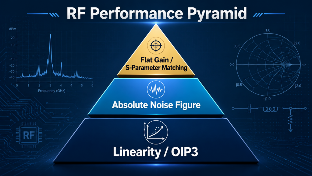
The base of the pyramid is linearity (IIP3/OIP3), not noise. If the amplifier is directly pushed into the compression region in the face of high-power interference signals, causing the intermodulation noise floor to soar by 10dB, then your nominal NF of less than 0.3dB is meaningless. The middle layer is the absolute noise figure optimization, but this must be built on a solid foundation of high IP3 topology. In the case of the spire, the flat gain distribution is controlled in order to prevent overloading of the subsequent downconverter or ADC stages.
Design Of L-Band Low Noise Amplifier For GNSS And Satellite Receiver
When deploying an l band low noise amplifier near an active source, a high linearity topology must be applied, otherwise the receiver will be instantly desensitized. Signals from GPS and GNSS constellations are woefully weak (typically below -125 dBm). When these receivers are integrated into the hardware of an IoT device or aerial telemetry system, they tend to be crowded with high-power telemetry or cellular transmitters on the physical PCB layout.
Overcoming 2.4 GHz Wi-Fi Desensitization in L-Band
Hanging a SAW filter directly in front of the LNA to hard carry 2.4 GHz interference, which directly wastes the sensitivity of the system on the physical level. To be honest, even if the insertion loss of the pre-filter is only 0.1 dB, it will directly add 0.1 dB to the total noise figure of the system. Friis formula does not tell you human feelings. The solution verified by our hardware is to place a high OIP3 LNA directly at the antenna feed line, followed by a high Q cavity or ceramic filter. This gameplay allows the L-band amplifier to absorb 2.4 GHz of out-of-band energy without saturation, preserving the original signal-to-noise ratio before the signal enters the filter.
2.4 GHz Low Noise Amplifier Performance In High Density ISM Hardware
The selection of 2.4 ghz low noise amplifier for Wi-Fi 6/7 or UAV control links is a great test of the ability to match S11 and S22 impedance under complex PCB stacks. The reason why high-density networks lose packets is mainly because the physical layer sensitivity of the receiving node is too bad. Don’t let the firmware team check the code back when you encounter packet loss.
Microstrip line via traps: Why the NF on the spec is lying
Hardware teams often find that their measured noise figure is 0.5 to 1.0 dB worse than the target value, mostly because they blindly believe in the Datasheet of semiconductor manufacturers. You know, fab data is measured directly on the die or reference board with accurately calibrated RF probes. But the real FR4 or Rogers board in your hand is full of heat dissipation vias, RF routing pads and solder paste, all of which will introduce parasitic inductance. This inductance, which is not modeled, directly changes the optimal source impedance (Gamma Optimum) required to achieve the lowest noise. After doing this for a long time, you will know that it is the right way to honestly and practically Keysight tools such as ADS or HFSS to do 3D electromagnetic simulation for specific via hole transitions on the board, and then deliberately fine-tune the input matching inductance to compensate for parasitic effects caused by the physical board layout.
Application Of C- Band Low Noise Amplifier In Deep Space Telemetry
The most important thing about integrating c band low noise amplifier into a satellite ground station or synthetic aperture radar (SAR) is phase stability and extreme survivability at extremely high incident power. Deep space telemetry operating in the 4 to 8 GHz range needs to capture weak signals reflected from orbital debris or planetary surfaces, which requires hardware that must not drift in parameters even under extreme temperature fluctuations.
GaN-on-SiC Contrast GaAs pHEMT: Kill the Front End Limiter
Silicon carbide-based gallium nitride (GaN-on-SiC) has essentially replaced the traditional gallium arsenide (GaAs)pHEMT in next-generation C- band receiver designs. Older GaAs LNAs must have a PIN diode limiter at the input to prevent burnout by stray radar pulses. But this limiter will impose a mandatory 0.3 to 0.5 dB insertion loss. In contrast, GaN-on-SiC structures are inherently capable of stiffening up to 5 watts of continuous wave (CW) input power without degradation. Directly unplugging the physical limiter can save that 0.5 dB loss from the cascade noise figure, which is equivalent to doubling the effective receive sensitivity immediately for deep space applications.
2025 Lab Test Data: Cross-Band Interference Suppression
Speaking with real data, the actual measurement can help you find out the precise threshold for out-of-band frequency breakdown receiver integrity. We measured L-band and C- band performance degradation by tapping a +10 dBm 2.4 GHz interferer directly into the signal path of three different LNA architectures.
| LNA Technology Type | Jamming Frequency (2.4 GHz Input) | Target Band (L/C Band) | Effective NF Post-Jamming | OIP3 Rating |
| Traditional GaAs (L-band) | +10dBm Jam | L-band | NF rises to 4.5dB | 22 dBm |
| Advanced GaN-on-SiC (C-band) | +10dBm Jam | C-band | NF stays at 0.4dB | 38 dBm |
| Hybrid pHEMT | +10dBm Jam | 2.4 GHz | NF 0.6dB | 34 dB |
In the face of such a violent saturation attack, the GaN architecture still keeps the noise figure at 0.4 dB. On the other hand, GaAs was blocked directly, the operating noise soared by more than 400, and the target frequency was completely submerged.
Technical FAQ (People Also Ask)
What Causes 2.4 GHz Low Noise Amplifier Desensitization?
Desensitization occurs when a strong out-of-band signal (such as a nearby 5 GHz transmitter or cellular band) forces the amplifier into the non-linear region of operation. This will produce intermodulation products, directly pull up the bottom noise, the already weak 2.4 GHz target signal to cover up. Replacing an LNA with a high output third-order intermodulation intercept point (OIP3) can effectively prevent the amplifier from entering the compression state prematurely.
Can amplifier handle C- band signals?
No way. The impedance matching of L-band amplifiers is usually optimized for maximum gain and minimum noise between 1 GHz and 2 GHz. If you force the C- band (4-8 GHz) signal to feed it, it will only lead to huge signal reflection (S11 is horrible) and serious gain roll-off. This amplifier is basically a piece of scrap metal when facing high frequency bands.
Why replace GaAs with GaN in c band low noise amplifier?
Compared with gallium arsenide (GaAs), gallium nitride (GaN) can withstand much higher input power without physical damage. Because of this “rough skin” characteristics, designers can directly put the input of the RF limiter to remove. the limiter is absent, its inherent insertion loss disappears, which is tantamount to directly optimizing the overall absolute noise figure of the system.
How does the PCB layout affect the LNA noise figure?
To achieve minimum noise, the required source impedance (Gamma Opt) is extremely sensitive to parasitic inductance. Those poorly designed PCB traces, pads with mismatched sizes, and perfunctory RF ground vias will pull the impedance away from the optimal point. The result is that the actual hardware noise figure you make is much worse than the level that the chip can theoretically achieve.
Should the filter be placed in front of or behind the LNA?
Placed behind the LNA, this is the iron law that preserves the sensitivity of the system. Any component with insertion loss (such as a filter), as long as you dare to put it in front of the LNA, its loss will be added to the total noise figure of the system. Unless the interference signal is strong enough to directly burn the amplifier physically or cause it to enter a permanent saturation state, never hang a filter in front of the LNA.