 Neditek
Coaxial Low Noise Power & Pre Amplifiers: 2026 Specs
Selecting the wrong low-noise amplifier (LNA) chip or failing to properly match a plug and play coaxial module can severely degrade the system’s signal to noise ratio (SNR), driving your project budget sharply upward. Many hardware integration failures stem from engineers blindly chasing high gain while neglecting to assess the 1-dB compression point (P1dB); or from misapplying low-noise amplifiers like the LNA 10 in heavily interfered with test environments; or, alternatively, from improper cascading of the low noise front end amplifier with downstream stages. In many cases, hidden impedance mismatches are quietly draining your engineering man-hours and eroding your return on investment (ROI).
We recommend carefully reviewing the following nine common hardware integration pitfalls to immediately close the “budget loopholes” in your project.
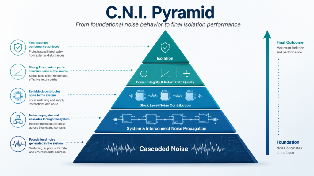
C.N.I. LNA Selection Pyramid: A Hardware Integration Framework
Many engineers waste weeks troubleshooting bit error rate (BER), ultimately because they evaluate the LNA’s parameters in isolation. Before placing a purchase order, why not try using our proprietary “C.N.I. Selection Pyramid” to conduct a comprehensive component evaluation?
C- Cascaded Noise Priority: The first-stage active device determines the overall system noise floor. You must remember that the front-end chip accounts for more than 90% of the system’s sensitivity.
N-Non-linear Headroom: If the signal is clipping, no amount of gain will make it any better. Be sure to thoroughly evaluate the OIP3 (third-order intercept point) to ensure your signal remains undistorted.
I-Impedance and Isolation: Die level chips have extremely stringent requirements for 50 ohm transmission lines. In contrast, coaxial modules, with their physical shielding enclosure, can resolve this issue almost instantaneously.
9 Fatal Integration Mistakes That Are Ruining Your LNA Investment Returns
Mistake 1: Treating the bare-die LNA chip as a direct drop-in replacement for the module.
Die-level requirements for PCB routing, thermal vias, and RF shielding verification are extremely stringent. Procurement staff often assume that spending just 5 yuan on a chip will allow them to use it right away—only to end up having to shell out $5,000 in engineering labor to tackle parasitic oscillation issues. For the test laboratory to achieve plug-and-play operation, it must be equipped with a low-noise coaxial amplifier. The coaxial shield effectively prevents external electromagnetic interference (EMI) from degrading your vector network analyzer’s (VNA) baseline measurement data.
Mistake 2: Misuse of the LNA’s 10 dB noise figure specification.
Without an intermediate bandpass filter, directly connecting the LNA 10 low noise amplifier to the antenna output is tantamount to rolling out the red carpet for interference, inviting severe out of band disturbances. The core metric that deserves the closest attention here is “out-of-band suppression.” Broadband modules like the LNA 10 operate on a “take all” principle: they amplify not only the signal from the local cellular base station but also that of nearby Wi Fi routers. Be sure to insert a high-Q filter before the gain stage to preserve your dynamic range.
Mistake 3: Ignoring the input-end return loss
Datasheets typically specify the noise figure (NF) at 50 ohms, but in practice, how many antennas are truly perfect 50 ohm loads? If the amplifier’s input voltage standing wave ratio (VSWR) is poor, the noise figure will degrade exponentially. Therefore, when selecting components, prioritize amplifiers that come with built-in matching networks and, if possible, avoid models that require a large number of external passive components.
Mistake 4: Overloading the low-noise preamplifier stage
Injecting a strong signal directly into an extremely sensitive low-noise preamplifier is like flooring the accelerator and driving it straight into the saturation region. System integrators often fail to account for the maximum input power (Pin MAX). Once the preamplifier reaches its 1-dB compression point, the generated harmonics will directly contaminate the entire data stream. If the strength of your source signal fluctuates, be sure to insert a variable attenuator in series.
Mistake 5: Blindly cascading low-noise power amplifiers
Without an interstage isolator, directly connecting the preamplifier to the low-noise power amplifier will invariably result in severe intermodulation distortion. Fluctuations in the input impedance of a power amplifier can cause energy to be reflected back to the output of the preamplifier. The IP3 levels of the two stages must be properly matched, and the power amplifier’s P1dB must significantly exceed the output power of the preceding stage.
| Specification | Low Noise Pre-Amplifier | Low Noise Power Amplifier |
| Typical Gain | Optimized for high sensitivity and low noise to capture weak signals. | Optimized for driving higher power levels in cascaded setups. |
| Max P1dB | Lower threshold (Must strictly monitor Pin MAX to avoid hitting the 1dB compression point and generating harmonics). | Must be significantly higher than the preceding Pre-Amplifier’s output power. |
| Target IP3 | Matched to the subsequent Power Amplifier’s IP3 level. | Matched to the preceding Pre-Amplifier’s IP3 level to prevent massive intermodulation distortion. |
| Primary Use Case | First-stage amplification of highly sensitive, fluctuating source signals (requires a variable attenuator). | Cascaded final-stage amplification (requires an inter-stage isolator to prevent energy reflection). |
Mistake 6: Neglecting thermal noise drift in high-density systems
Since rising temperature intensifies the thermal motion of electrons, the background noise naturally increases in tandem. Today’s hardware systems are highly dense, with numerous RF chips crammed into small enclosures, making localized overheating an everyday occurrence. An LNA that achieves a noise figure of 0.8dB at 25°C may easily degrade to 1.5dB at 85°C. When setting up a continuous-wave (CW) test environment, be sure to specify a coaxial enclosure equipped with a heat sink.
Mistake 7: Forgetting about Friis’s formula
Many systems fail because engineers don’t think to add a high-gain amplifier until they reach the end of the signal chain, hoping it will compensate for the noise introduced at the front end.
Friis (Friis) formula has long been clear: the receiving link in the leading components, directly determines the life and death of the whole system bottom noise. As long as you put the device with the best quality and lowest noise in your hand next to the signal source, it will be stable.
Mistake 8: Make do with unshielded test fixtures
If alligator clips and jumpers that do not even have a shielding layer are used on the test bench to test the die amplifier, the measured noise figure (NF) data is absolutely impossible to see. RF test engineers must stick to it: an honest and practical calibrated torque wrench with high-specification SMA or N-type cables. When doing the most fatal S-parameter verification, a pre-matched coaxial shell can help you completely uproot the error caused by the ground loop.
Mistake 9: Put the power supply rejection ratio (PSRR) on deaf ears
The switching power supply will directly pour high-frequency switching noise into the amplifier along the DC bias line. It should be understood that LNA chips are extremely sensitive to voltage ripple. The power line must pass through a low dropout (LDO) linear regulator 1 times, and the cost on the decoupling capacitor cannot be saved. If you dare to ignore PSRR, your amplifier minutes into a “noise generator”.
Real-World Case: ROI (Return On Investment) Of Bare Die Versus Coaxial Modules
In a 5G macro base station test bed system integration project in the 3 quarter of 2024, a hardware team replaced the original bare chip LNA chip with the 1 coaxial low noise amplifier calibrated before leaving the factory. At the beginning of the die, the noise figure was abruptly deteriorated by 2.5dB due to EMI interference in the laboratory and parasitic effects of wiring. Later, the grind was upgraded to a coaxial module. NF was steadily lying at 1.1dB and the curve was very flat. The most immediate benefit is that 45 hours of debugging and troubleshooting time are saved on the spot. After conversion, each test rack directly cuts the research and development cost of 6500 US dollars.
LNA Device Application Matrix Understood By 1 Chart: What Scene To Pick What Goods
Telemetry system below 1GHz: honest and practical discrete LNA chip, equipped with specially customized high Q value inductor to do impedance matching.
Laboratory VNA calibration: Decisive high-isolation coaxial low-noise amplifier.
Receiver front end: must be closely shielded on the low noise preamplifier, so as to catch the extremely weak echo.
Transmitter driver stage: select the integrated low-noise power amplifier, raise the signal level before entering the final power amplification, and at the same time hold down the phase noise to prevent it from rising.
Everyone Is Asking (FAQs)
Q: What is the difference between a low-noise preamplifier and an ordinary LNA?
A: The low-noise preamplifier is specially tailored for the “first 1 stage” of the receiver link. Its ultimate mission is to keep the noise figure to an absolute minimum. In order to achieve extreme sensitivity, some high output power is often sacrificed. In contrast, the ordinary LNA is more like a “water master”, generally looking for a balance between noise figure, large dynamic range and linearity.
Q: How do you measure the noise figure of a low-noise amplifier like LNA-10?
A: You have to pull out a calibrated noise figure tester, or a spectrum analyzer with a noise source. Before starting the test, ENR (super-noise ratio) calibration is an essential step. The most critical point: be sure to tighten the coaxial cable with a torque wrench, otherwise the insertion loss will fluctuate a little, and all the work in front of you will be done in vain.
Q: Can I use a coaxial low-noise amplifier to transmit signals?
Answer: Don’t do such a stupid thing. Coaxial LNA is born to eat the bowl of rice of receiving (Rx) link and can only serve weak signals at the microvolt level. If you overlord hard bow, the high-power transmission (Tx) signal into the filling, inside those delicate transistors will burn out in an instant, completely scrapped.
Q: Why does my low-noise power amplifier cause distortion in the RF signal?
Answer: Once distorted, it means that the input signal has broken through the linear working area of the amplifier. Take the output power of your system and match the P1dB and IP3 indexes of the amplifier. If the input signal is too “punched” (the level is too high), the amplifier will cut off the peak like a chop, creating serious intermodulation distortion.
Q: VSWR (standing wave ratio) is too poor, what consequences will it cause to LNA chip?
A: A poor VSWR means that the impedance is not well matched, and the RF energy will bounce back to the input of the chip. This kind of “tempering” will not only directly destroy your noise figure and eat the actual gain; when the situation is serious, it will even make the amplifier completely out of control and shock.
Q: Why is the LNA system that I cascade out so much noise?
A: The high probability is that you have blocked a noisy device in front of the main LNA, or you have not given enough gain in the 1 stage. Remember this iron law: the gain of the 1-stage amplifier must be large enough to suppress the noise made by all components behind the entire signal chain.
Q: Does my coaxial module require an external DC block?
A: You have to go through the specific data manual (Datasheet) for this. At present, many high-end coaxial modules have integrated DC blocking capacitors in RF IN and RF OUT ports. If your head iron is connected to the port without direct current, your test equipment will be short-circuited on the spot.