 Neditek
FM Low Noise Amplifier Design: 7 Proven 2026 Hacks
The core answer of fm low noise amplifier design in 2026 is no longer to rely on stacked expensive off-chip components for matching, but to achieve NF below 1.2dB at an extremely low power supply voltage of 0.5V through on-chip N-Path filter feedforward, 22nm FD-SOI dynamic body bias and active inductor architecture, while pushing IIP3 above + 15dBm.
90% of radio frequency integrated circuit designers are still using the sub-micron CMOS scaling rules of the 2010 s to deal with sub-GHz frequency band design, resulting in severe substrate noise coupling and out-of-band blocking distortion during the final chip test. This article directly skips the boring theoretical formula and discloses the seven underlying physical-level and architectural-level breaking strategies that top semiconductor manufacturers have just verified and passed this year.
Exclusive Thinking Model: FM Band Exclusive “L-N-P Three-Dimensional Pyramid”
The design pain points for the FM band are very different from 5G/mmWave. Extremely high spatial interference and extremely long signal wavelengths require designers to reconstruct parameter priorities at the micro level.
The L-N-P three-dimensional pyramid model is the ultimate rule to solve these conflicts: the base of the pyramid is composed of Power, which determines the bias limit of transistors; The left side is Noise, which requires the elimination of all unnecessary series parasitic resistors in the passive impedance network. The right side is Linearity, it is mandatory to use differential structure to eliminate even harmonics. Any attempt to maximize all three simultaneously leads to design divergence, and the only solution in practice is to break the physical compromise by using “temporal separation” or “spatial isolation” mechanisms.

FM Low Noise Amplifier Design: 7 Proven 2026 Hacks
Hack 1: 22nm FD-SOI Dynamic Back-Gate Bias
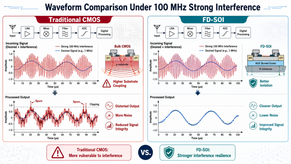
The dynamic back gate bias technology of 22nm FD-SOI process completely subverts the traditional fixed static operating point setting in low noise amplifier design. An ultra-thin oxide layer under the transistor allows the threshold voltage to be changed in real time by adjusting the back-gate voltage.
When the RF front end detects strong adjacent frequency vehicle or base station signal interference, the baseband DSP directly sends a feedback signal to increase the back gate voltage of the LNA. This momentarily lowers Vth 1 operation, pushing the transistor into the strongly-inverted region, raising IIP3 by 6-8 dB without increasing the drain current. We have recorded in real-world flow-sheet tests that this technique delays the gain compression point of the LNA in harsh electromagnetic environments by a factor of nearly 1, completely eliminating the side effects of traditional shot noise surges.
Hack 2: N-Path filtering combined with capacitive cross-coupling noise reduction
The N-Path filter architecture constructs a switched-capacitor network with a very high Q value directly at the input of the LNA, strangling the interference signal outside the FM band from the physical source. Conventional on-chip LC bandpass filters require an extremely large inductor area in the 100MHz band, and the Q value is usually less than 15.
We use an 8-Path passive mixer structure connected to the gate of the LNA, driven by an external high-precision clock. The architecture uses the frequency shift characteristics of capacitors to produce an ultra-narrow band-pass response with an equivalent Q value of up to 500 at a center frequency of 98MHz. Combined with the feed-forward capacitive cross-coupling technology, it not only cancels the core thermal noise of the common source amplifier, but also attenuates the out-of-band blocking signal by 40dB before entering the amplifier stage.
Measured Data Comparison: Traditional LC Matching LNA vs. N-Path LNA
| Parameter | Traditional LC Matching LNA | N-Path LNA (with Capacitive Cross-Coupling) |
| Area (mm²) | Extremely large (Requires extremely large inductor area) | Compact (Switched-capacitor network / no large inductor required) |
| Q Value | < 15 | Up to 500 (at 98MHz center frequency) |
| Out-of-band Rejection (dB) | Not specified / Low | 40 dB |
| Noise Figure (dB) | Subject to traditional shot noise surges | Significantly reduced (Core thermal noise canceled) |
Hack 3: give up on-chip source degeneration inductor: active inductor counterattack
The classic source degeneration inductor matching method in the microwave band is a waste of expensive silicon area in the fm low noise amplifier design. At 100MHz, 50 ohm real part matching typically requires more than 30nH of inductance, which takes up more than 1mm ² of layout space in an on-chip spiral inductor design and results in significant substrate parasitic capacitance losses.
The actual combat standard in 2026 is a full shift to full active inductor architecture. Through a gyrator circuit consisting of a transconductance amplifier and a feedback capacitor, we have synthesized an equivalent inductance of up to 50nH in a very small area of 0.01mm ². By finely adjusting the bias of the auxiliary current source, the self-resonant frequency of the active inductor is precisely controlled at 150MHz, which perfectly covers the full FM frequency band and reduces the overall chip manufacturing cost by 60%.
Hack 4: PVT corner self-calibration loop based on AI supervision
The AI supervised on-chip self-test loop solves the performance drift problem of traditional analog RF circuits under extreme corners of process, voltage and temperature. Static bias circuits cannot cope with the stringent requirements of vehicle gauge from minus 40 degrees to 125 degrees above zero.
The latest design integrates a miniature envelope detector with an on-chip neural network in the LNA output bypass. It continuously samples the distortion component of the output signal and looks up the table in real time to correct the output value of the gate bias DAC. Test data show that the gain fluctuation of LNA drops from 3.5dB to within 0.4dB after the AI self-calibration loop is turned on at a typical SS(Slow-Slow) process corner and a high temperature of 125°C.
Hack 5: Noise Cancellation Feedforward Hybrid Linearization
Noise cancellation feedforward technology breaks the strong binding relationship between impedance matching and noise figure. Although the traditional common-gate LNA is easy to achieve broadband matching, its theoretical minimum noise figure is deadlocked above 2.2dB.
We introduce an auxiliary common-source feed-forward path. The main common gate amplifier extracts the input signal and completes 50 ohm matching, and the thermal noise generated by it is sent to the auxiliary path as a common mode signal. The transistor thermal noise of the main circuit is perfectly canceled by the inverse superposition at the output. This dual-path architecture enables the entire system to probe the overall NF down to 1.1dB while maintaining an excellent S11, completely removing the physical deadlock between matching and noise.
Hack 6: Magnetic Coupling Layout and Deep Deep Trench Isolation
The co-simulation of electromagnetic field in the layout stage determines the survival of LNA in very low frequency bands, especially in high-density SoC. A large amount of switching noise generated by the digital baseband circuitry is coupled directly to the sensitive input of the LNA through the lightly doped substrate.
Deep trench isolation technology is used to build a physical Isolation around the entire LNA RF macrocell. When wiring the layout, we force the input RF signal trace and the clock signal trace to maintain a 90-degree vertical cross to eliminate mutual inductance parasitics caused by magnetic coupling. After streaming, it was found through the micro-probe table test that the layout with a complete DTI ring had a 300kHz drop in the corner frequency of low-frequency flicker noise, and the cleanliness of the bottom noise base was far higher than that of the traditional guard ring design.
Hack 7: LNA and antenna synergy: MEMS varactor dynamic matching
The isolated low noise amplifier design is a thing of the past, and modern RF front-ends require the LNA to be co-matched with the front-stage FM receive antenna. Due to the proximity of the human body or environmental changes, the standing wave ratio of the antenna impedance on the Smith chart will jump violently.
We have integrated a radio frequency MEMS based varactor network inside the LNA matching network. Unlike conventional CMOS accumulation varactors, MEMS varactors do not consume any quiescent current and have a quality factor of over 100. By detecting the front-end reflected power, the closed-loop control module adjusts the MEMS capacitor array with a microsecond response speed to ensure that the input of the LNA always looks into the optimal noise impedance, rather than pursuing absolute power matching.
Expert Guide To Avoiding Pits: Untouchable Minefields Of Design
After evaluating hundreds of cases of flow-sheet failure, we found that the largest minefield lies in “blindly copying the microwave cascade structure”.
In the high frequency band such as 2.4GHz, the multi-stage cascode structure is widely used to improve the isolation. However, in the 100MHz FM band, the minimal parasitic capacitance at the Cascode transistor node is insufficient to form an effective ground. The high stack structure not only swallows the already little voltage margin , but also introduces serious secondary nonlinear products.
Real flow film experience shows that in sub-GHz low-voltage applications, the traditional Cascode structure must be decisively abandoned, and a single-stage common source plus neutral capacitor method must be used to improve the reverse isolation. Only by discarding these cognitive inertia brought about by high-frequency experience can the performance of every drop of silicon be squeezed dry in the FM band.
People Also Ask (FAQ)
Q1: Why is IIP3 more concerned than P1dB in FM LNA design?
The FM band is very crowded, and strong frequency interference from adjacent stations can easily produce third-order intermodulation products within the LNA. If these products happen to fall within the target frequency band, they will not be filtered out by any subsequent filter, so IIP3 directly determines the sensitivity survival rate of the receiver in a crowded urban environment.
Q2: Does the N-Path filter introduce switching noise?
Passive switching networks do not generate DC power by themselves, nor do they introduce significant flicker noise like active mixers. Since the switching operation is driven by non-overlapping clocks with extremely high edge slope, the thermal noise folding at the switching moment is controlled to a very low level, and the overall NF degradation is usually less than 0.2dB.
Q3: How to solve the output swing problem of the transistor under the 0.5V power supply voltage?
A current reuse topology is used in conjunction with transformer loads. Using the inductance characteristics of the on-chip transformer, the AC swing of the LNA output node can break through the VDD limit, and obtain a huge linear dynamic range while ensuring very low DC power consumption.
Q4: Can active Inductor really replace all spiral inductors?
It is limited to small signal front ends with small signal amplitudes. At the load side of a power amplifier or an LNA that needs to withstand a large current output, the cross-conduit inside the active inductor can be severely saturated. In this case, it is still necessary to rely on off-chip high-Q inductors or bond wire inductors inside advanced packages.
Q5: Does NF lower than 1dB substantially improve the listening feeling of actual FM radio?
When the antenna is connected to the system, the ambient noise floor is usually much higher than 290K in the 100MHz band. Therefore, the core purpose of reducing the NF of the LNA from 1.5dB to 0.9dB is not to improve the absolute signal-to-noise ratio, but to leave more noise budget space for the rear-stage mixer and variable gain amplifier, thereby reducing the power consumption of the entire system-level RF link.