 Neditek
GaN HEMT Cross Section: Revealing Internal Topologies
The Core Anatomy Dictating Device Limits
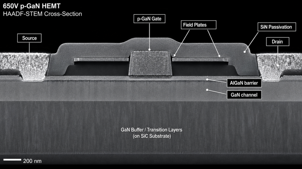
The physical topology of a GaN HEMT directly dictates its electrical limits, where a standard cross section exposes the precise AlGaN/GaN heterojunction driving the 2DEG channel, the carbon-doped buffer layers, and the exact geometric overlap of the source-connected field plates. Extracting precise dimensional data from these internal layers separates a robust 650V power switch from one plagued by dynamic Ron degradation and premature dielectric breakdown. Most reverse engineering reports stop at measuring baseline layer thicknesses without probing the atomic lattice mismatch. We will tear down the exact polarization forces shaping the GaN HEMT band diagram, expose hidden carbon doping traps within the buffer layer, and detail the specific FIB (Focused Ion Beam) sample preparation pitfalls that continuously ruin failure analysis (FA) results for engineering teams.
The DEP Framework for Reverse Engineering GaN Structures
Process integration engineers require a systematic method to evaluate competitor topologies. The DEP (Dielectric-Epitaxy-Plate) Analysis Framework provides a strict procedural standard for extracting actionable intelligence from any GaN HEMT cross section.
Dielectric Passivation Mapping
Dielectric mapping defines the first pillar of the framework. Analyzing the Silicon Nitride (SiN) or Aluminum Oxide (Al₂O₃) layers under high magnification reveals step-coverage integrity. Voids or micro-cracks at the field plate corners indicate a high probability of electric field crowding, directly correlating to catastrophic breakdown during hard-switching events.
Epitaxial Interface Profiling
Epitaxial profiling targets the atomic reality of the semiconductor layers. Energy-Dispersive X-ray Spectroscopy (EDX) scans across the AlGaN/GaN boundary map the exact aluminum mole fraction gradient. A sharp transition ensures strong electron confinement, while a diffused gradient suggests poor thermal management during MOCVD epitaxial growth, leading to a degraded 2DEG density.
Field Plate Geometry Extraction
Field plate geometry dictates the device’s voltage blocking capability. Engineers measure the lateral extension (L_FP) and the vertical dielectric thickness standing between the source-connected plate and the gate edge. Millimeter-level misalignments here drastically shift the peak electric field away from the gate edge, heavily impacting the off-state leakage current.
Decoding the Exact GaN HEMT Structure Layer by Layer
Every layer in the GaN HEMT structure serves a dedicated physical purpose, reacting dynamically under high voltage stress.
Substrate and Nucleation Layer Dynamics
The mechanical foundation dictates the strain propagation through the entire device. Silicon (Si) substrates remain the industry standard for cost efficiency, but the significant lattice mismatch with GaN requires a highly engineered Aluminum Nitride (AlN) nucleation layer. Cross-sectional Transmission Electron Microscopy (TEM) routinely exposes threading dislocations initiating at this AlN/Si boundary. Competitor teardowns show that superior devices utilize complex superlattice structures (e.g., alternating AlGaN/GaN layers) to trap these dislocations before they penetrate the active channel.
The Buffer Layer and Carbon Doping Trap Profile
Managing vertical punch-through voltage requires heavy carbon doping in the GaN buffer layer. Energy-filtered TEM (EFTEM) cross sections expose the exact concentration profile of these carbon atoms. High Vds stress injects hot electrons deep into this layer, where they become trapped by the carbon sites. This specific mechanism causes current collapse and dynamic Ron degradation. Engineers analyzing device failures must profile this buffer region to determine if the carbon doping gradient is too aggressive near the channel interface.
GaN HEMT Band Diagram: Visualizing the Polarization Field
Spontaneous and piezoelectric polarization fields strictly govern the operational physics of the GaN HEMT band diagram.
Strain-Induced Piezoelectric Effects Driving the 2DEG
The lattice constant mismatch between the thin AlGaN barrier and the thick GaN channel generates immense tensile strain. This physical strain forces a piezoelectric polarization vector that aligns with the spontaneous polarization of the wurtzite crystal structure. The resulting positive sheet charge at the interface aggressively bends the conduction band downward. Electrons populate this triangular quantum well, forming the 2-Dimensional Electron Gas (2DEG) with sheet densities often exceeding 10¹³ cm⁻². Any relaxation of the AlGaN layer thickness directly flattens the band diagram, destroying the 2DEG conductivity.
p-GaN Gate Modulation for Enhancement Mode Devices
Normally-off (Enhancement mode) operation demands a severe alteration of the local band diagram directly under the gate metal. Inserting a magnesium-doped p-GaN layer between the Schottky metal and the AlGaN barrier lifts the conduction band above the Fermi level at zero gate bias. This completely depletes the 2DEG in the channel region below the gate. Applying a positive gate voltage (Vgs) pulls the band structure back down, re-establishing the quantum well and allowing electron flow. Cross-sectioning this specific p-GaN region requires extreme precision, as the exact thickness and sidewall angle of the p-GaN layer dictate the threshold voltage (Vth) stability.
Expert Pitfall Guide: Avoiding FIB Artifacts in FA
Focused Ion Beam (FIB) milling destroys the precise epitaxial boundaries required for accurate failure analysis if left unpolished.
Standard Gallium-based FIB preparation implants heavy Ga⁺ ions directly into the exposed cross-section sidewalls. This contamination creates amorphous layers that mimic actual structural defects under a TEM. Reverse engineering analysts frequently misinterpret these FIB-induced artifacts as native electron traps or structural degradation caused by electrical stress.
Low-voltage Argon ion milling must act as the final polishing step. Broad-beam Argon milling at energies below 1 keV removes the amorphous gallium-rich damage layer, restoring the crystalline reality of the cross section. Teams skipping this final polish consistently report inaccurate AlGaN thicknesses and false interface roughness data, rendering their entire reverse engineering effort useless.
Real-World Teardown Data: 650V E-Mode Anomalies
Laboratory teardowns of competing 650V E-mode devices reveal striking discrepancies in field plate execution.
We subjected two separate commercially available 650V GaN HEMTs to repetitive hard-switching at 400V. Device A suffered a catastrophic gate rupture after 100 hours, while Device B passed the 1,000-hour mark with zero Ron shift. Subsequent cross-section analysis utilizing the DEP framework exposed the root cause.
Device A exhibited a 5-nanometer structural offset between the p-GaN gate edge and the primary source-connected field plate. This minute gap caused massive electric field crowding inside the SiN passivation layer, leading to dielectric breakdown. Device B employed a stepped, multi-level field plate topology that perfectly distributed the electric field peak away from the vulnerable gate corner, proving that sub-micron geometric control dictates macroscopic reliability.
Teardown Metrics: 650V E-Mode GaN HEMTs (Device A vs. Device B)
| Metric | Device A | Device B |
| Field Plate Length / Topology | Features a 5-nanometer structural offset between the p-GaN gate edge and the primary source-connected field plate. | Utilizes a stepped, multi-level field plate topology. |
| Passivation Thickness | Not explicitly specified (Composed of SiN dielectric material). | Not explicitly specified. |
| Ron Degradation (%) | N/A (Test terminated due to catastrophic failure at 100 hours). | 0% (“Zero Ron shift” after passing the 1,000-hour mark). |
| Failure Mechanism | Catastrophic Gate Rupture: The 5-nm gap caused massive electric field crowding inside the SiN passivation layer, leading to dielectric breakdown. | None (Passed): The multi-level geometry perfectly distributed the electric field peak away from the vulnerable gate corner. |
FAQ
How do you determine the 2DEG density from a GaN HEMT cross section?
Direct visual measurement of 2DEG density from a standard cross section is impossible. Analysts extract the exact AlGaN layer thickness and Aluminum composition via EDX/EELS mapped from the cross section, then input these geometric and material values into Poisson-Schrödinger solvers to calculate the theoretical sheet charge density dictated by the polarization band diagram.
Why is carbon doping visible in GaN HEMT buffer layer cross sections?
Carbon doping acts as a deep acceptor trap to compensate for unintentional background donors (like oxygen or silicon) in the GaN buffer. Secondary Ion Mass Spectrometry (SIMS) combined with cross-sectional mapping reveals this carbon gradient, which is deliberately engineered to prevent high-voltage punch-through leakage from the drain to the substrate.
What is the role of the AlN exclusion layer in the GaN HEMT structure?
An ultrathin Aluminum Nitride (AlN) spacer layer (usually 1-2 nm) is frequently inserted precisely between the AlGaN barrier and the GaN channel. Cross sections under high-resolution TEM reveal this layer, which serves to drastically reduce alloy scattering. It physically separates the 2DEG electrons in the channel from the rough interface of the ternary AlGaN alloy, maximizing electron mobility.
How does a recessed gate structure alter the band diagram?
Recessed gate architectures involve physically etching away a portion of the AlGaN barrier directly beneath the gate metal. This deliberate thinning weakens the piezoelectric polarization locally, pulling the conduction band up to intersect the Fermi level. The result is a highly localized depletion of the 2DEG, forcing the device into normally-off (enhancement mode) operation without needing a p-GaN layer.
Why do failure analysis engineers look for voids in the SiN passivation?
Silicon Nitride (SiN) acts as the primary defense against surface state trapping and moisture ingress. Cross-sectional SEM scans that detect microscopic voids in this layer indicate weak dielectric strength. High electric fields concentrate around these physical voids, accelerating electron injection into the passivation and triggering irreversible dielectric breakdown during high-voltage switching.