 Neditek
PIN Diode vs Avalanche Photodiode: Key Performance Comparison
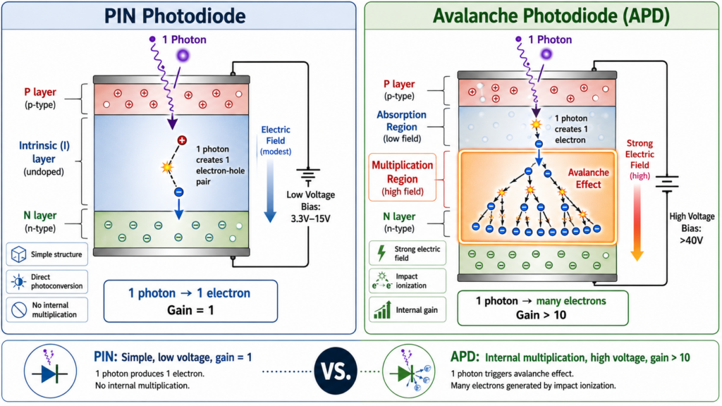
The fundamental difference between a pin diode vs avalanche photodiode lies in internal optical gain. PIN diodes operate with zero internal amplification (Gain = 1), delivering exceptional stability, ultra-low noise, and low-voltage operation for environments with strong optical signals. Avalanche photodiodes (APDs) utilize impact ionization to multiply charge carriers (Gain > 10), enabling single-photon level sensitivity for weak-signal detection, but demand complex high-voltage bias circuits and strict temperature regulation. Selecting the wrong photodetector will instantly wreck your power budget or severely bottleneck your system’s bandwidth. The breakdown below strips away the marketing jargon to expose the raw performance limits, actual deployment costs, and architectural trade-offs of both technologies.
The V.E.N.T. Selection Framework: Bypassing the Datasheet Trap
Engineers regularly select components based on ideal lab conditions, ignoring real-world environmental stress. Use the V.E.N.T. matrix to lock down your component choice before designing the PCB.
- V – Voltage Limits: PIN diodes run cleanly on standard 3.3V to 15V rails. APDs require dedicated high-voltage DC-DC converters to supply 40V to 200V+ to sustain the avalanche effect.
- E – Environmental Stability: PIN responsivity remains largely flat across broad temperature ranges. APD multiplication factors fluctuate violently with temperature changes, necessitating active cooling (TECs) or complex temperature-tracking bias circuits.
- N – Noise Floor: PIN diode receivers are limited by the thermal noise of the downstream Transimpedance Amplifier (TIA). APDs generate inherent “excess noise” due to the statistical nature of the avalanche process.
- T – Throughput (Bandwidth): PIN diodes dominate ultra-high-speed short-reach data paths (up to 100Gbps+ per lane) due to lower transit times. APDs excel in long-haul, lower-bandwidth applications where signal attenuation is the primary enemy.
Key Performance Metrics Face-Off
Every datasheet features specific test parameters. This section translates those isolated numbers into system-level performance impacts.
Sensitivity and The Multiplication Factor (M)
APDs physically multiply the incoming light signal before it hits the external circuitry. An APD absorbs a single photon and generates multiple electron-hole pairs, creating a multiplication factor (M) typically ranging from 10 to 100. This internal gain pulls weak signals directly out of the noise floor, making APDs mandatory for long-haul OTN (Optical Transport Network) links exceeding 80km. PIN diodes generate exactly one electron per absorbed photon. They rely entirely on external TIAs to boost the signal, which inevitably amplifies external circuit noise alongside the signal.
PIN Diode vs. APD Core Performance Metrics and Selection Parameters Comparison
| Performance Metric / Parameter | PIN Diode | Avalanche Photodiode (APD) |
| Typical Applications | Data center CPO, short-reach high-speed interconnects | Long-haul OTN, PON networks, weak signal detection |
| Internal Gain (M) | 1 (Generates exactly one electron per photon; no internal amplification) | 10 ~ 100+ (Internal gain via avalanche multiplication effect) |
| Bias Voltage | 3.3V ~ 15V (Runs cleanly on standard voltage rails) | 40V ~ 200V+ (Requires dedicated high-voltage DC-DC converters) |
| Main Noise Source | Thermal Noise (Originates from the downstream Transimpedance Amplifier / TIA) | Excess Noise (Inherent statistical noise generated by the avalanche process) |
| Sensitivity Level | Medium / Low (Relies entirely on external amplifiers to pull signal from noise floor) | Extremely High (Capable of weak signal and even single-photon detection) |
| Temperature Stability | High (Responsivity remains largely flat across broad temperature ranges) | Low (Multiplication factor fluctuates violently; requires active cooling/TECs or complex temperature-tracking bias circuits) |
| Maximum Bandwidth / Speed | Extremely High (Lower transit times; easily supports 400G/800G, up to 100Gbps+ per lane) | Limited (Restricted by avalanche build-up time; bound by the Gain-Bandwidth Product limit) |
Noise Profiles: Thermal Limitation vs. Excess Noise
APDs introduce a specific degradation metric known as the Excess Noise Factor (F). The impact ionization process inside an APD is unpredictable; not every electron multiplies perfectly. Pushing the bias voltage too high to increase gain actually degrades the Signal-to-Noise Ratio (SNR) because the excess noise scales faster than the signal. PIN diodes are free from excess noise. Their primary noise bottleneck is entirely predictable thermal noise (Johnson noise) originating from the terminating resistors and the first-stage amplifier.
Response Time and Bandwidth Ceilings
PIN diodes switch faster in dense, high-speed arrays. The thick intrinsic layer of a PIN minimizes junction capacitance, allowing modern InGaAs PIN photodiodes to comfortably handle 400G and 800G optical transceivers. APDs suffer from the “avalanche buildup time.” The process of charge carriers bouncing back and forth to create secondary electrons takes physical time, imposing a strict gain-bandwidth product (GBW) limit.
Expert Pitfalls: Field Failures the Industry Rarely Discusses
Junior hardware engineers frequently make critical miscalculations when choosing between an avalanche photodiode vs pin diode. Here are two field-tested realities.
The Thermal Runaway Trap
APD breakdown voltage (V_BR) has a positive temperature coefficient. A system calibrated perfectly at 25°C will fail completely at 65°C. At higher temperatures, the semiconductor lattice vibrates more, shortening the mean free path of electrons. You must apply higher voltage to maintain the same gain. If the bias circuit lacks a thermistor-driven compensation loop, an unexpected temperature drop will cause the fixed high voltage to exceed the new, lower V_BR, instantly destroying the APD through thermal runaway.
The Dark Current Penalty
Dark current acts as a persistent static hiss in your optical receiver. Because APDs amplify everything, they also amplify their own bulk dark current. In weak-signal applications like SWIR (Short-Wave Infrared) sensing, an improperly cooled APD will generate so much multiplied dark current that it completely masks the actual optical pulses, rendering the expensive sensor worse than a $2 PIN diode.
2026 Industry Application Splits
The boundary between these two components has hardened significantly due to distinct shifts in telecommunications and automotive architectures.
- Silicon Photonics & Datacenters (PIN Dominance): AI-driven datacenter interconnects strictly utilize arrays of high-speed PIN diodes. The density requirements of co-packaged optics (CPO) leave zero physical space for the high-voltage rails required by APDs.
- Next-Gen LiDAR & Deep Space (The SPAD Shift): While linear APDs were once the gold standard for automotive LiDAR, the industry is aggressively migrating to Single Photon Avalanche Diodes (SPADs) biased above the breakdown voltage (Geiger mode) to achieve true digital photon counting.
- FTTH and Long-Haul Telecom (APD Stronghold): Standard APDs remain the undisputed choice for 10G-PON and 25G-PON fiber-to-the-home networks, where compensating for passive optical splitter losses dictates high receiver sensitivity.
FAQ
Why is an APD more sensitive than a PIN diode?
An APD is more sensitive because it contains a specific multiplication region with a strong electric field. When light hits the photodiode, the generated electrons are accelerated to such high speeds that they knock additional electrons free from the semiconductor lattice, amplifying the signal internally before any external noise is introduced.
Can I replace a PIN diode directly with an Avalanche Photodiode?
Direct replacement is impossible. A PIN diode operates on low voltage (e.g., 5V) and requires a high-gain transimpedance amplifier. An APD requires a high-voltage supply (often > 60V), a temperature compensation circuit, and a completely different TIA specification to handle the multiplied signal and excess noise factor.
Is a PIN diode faster than an APD?
Yes. High-speed PIN diodes generally offer higher bandwidths than APDs. APDs are limited by avalanche build-up time—the physical delay caused by the multiplication process. PIN diodes only rely on carrier drift across the depletion region, making them the standard for > 40Gbps data communication lanes.
What is the dark current difference between PIN and APD?
An APD exhibits significantly higher dark current than a PIN diode. The primary reason is that the APD physically amplifies its own un-illuminated leakage current (bulk dark current) through the avalanche process, whereas a PIN diode only experiences the baseline thermal generation of carriers.
When should I avoid using an Avalanche Photodiode?
Avoid APDs when your optical signal is already strong, your power budget is strictly limited, or your system experiences drastic temperature fluctuations without the capacity for active cooling. Using an APD in high-light conditions forces you to lower the bias voltage, effectively reducing it to an expensive, underperforming PIN diode.