 Neditek
Low Noise Amplifier Vs Power Amplifier: Avoid 3 Mistakes
After contacting numerous industrial-grade Internet of Things and RF links at the bottom of smart factories, I found a very realistic data: about 70% of novice engineers will stumble when designing wireless links for the first time. It’s not because they don’t understand the basic definitions of LNA (low noise amplifier) and PA (power amplifier)-everyone knows that LNA amplifies weak signals at the receiving end, and PA pushes the power to the maximum at the transmitting end. What really makes them screw up is that the hard indicators of component isolation, linear margin and material limit are not handled properly. Once the design center of gravity is mixed up, the transceiver’s transmission distance and signal integrity will instantly collapse. Today, let’s talk about the 3 system-level pit that must be avoided when comparing LNA and PA.
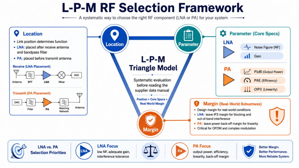
I Often Use The “L-P-M” Triangle Selection Model.
Before looking through the supplier’s data manual, there must be a systematic evaluation framework. I am used to using a set of “L-P-M (position-parameter-margin)” triangle model to card the specifications of the components. This method works well in real projects:
Location (link position): position determination function. The LNA must be attached to the back of the receive antenna and bandpass filter. And the PA, right in front of the transmit antenna.
Parameter (core parameters): LNA dead-stare noise figure (NF) and gain. PA value is the output 1dB compression point (P1dB), power added efficiency (PAE) and OIP3.
Margin (design margin): The beautiful data of the laboratory is one thing, and the real harsh environment performance is definitely discounted. The LNA has to leave enough IP3 margin to cope with out-of-band interference blocking. PA must leave a power back-off (power back-off) margin, otherwise it cannot withstand the linearity requirements of complex modulation such as OFDM.
Error 1: Dead-Eye Gain, But Fall Into The Trap Of Cascading Noise And Linearity.
In the actual selection, it is often seen that some people pick “high gain” pipes as soon as they come up, and they have not caught the real bottleneck of RF link budget.
Whether LNA can survive depends on the Friis formula for calculating cascaded noise figure. The first device on the link you receive directly determines the noise floor of the entire system. In my experience, if you add a high-loss switch or a cheap filter in front of the LNA, then no matter how beautiful the noise figure of your LNA itself is, the receiving sensitivity will be directly discarded. As long as there is an extra 1dB of insertion loss in front of the LNA, the total NF of the system will actually increase by 1dB. Remember to place the LNA as close to the antenna as possible.
On the PA side, the fight is a linear performance under complex modulation. Many purchasers have a misconception that looking at PA marked “30dBm P1dB”, they expect it to be able to play 30dBm 5G signals cleanly. The reality is that signals with extremely high peak-to-average ratio (PAPR) such as 64-QAM or 256-QAM will definitely clip severely at the P1dB point. You must honestly do a 6dB to 9dB “power back-off” from the P1dB point, otherwise the spectrum regeneration (spectral regrowth) and EVM (error vector magnitude) data will be extremely ugly.
Wrong 2: Wrong Semiconductor Materials In Modern Design
The traditional gallium arsenide (GaAs) is now still brainlessly used in all amplifier modules, which is long overdue and will completely screw up the thermal budget of your modern IoT device or 5G base station. The performance of different materials on LNA and PA can be said to be very different.
At present, in the PA market of high-power infrastructure, gallium nitride (GaN) is the absolute main force. GaN can work at a high pressure of 28V or even 48V, and can withstand extremely high heat density. It is estimated that silicon material will burn through at the same power. Especially in the Doherty architecture, GaN can provide extremely high PAE, which can exceed 50% at any time.
In turn, to do high integration of LNA, silicon germanium (SiGe) and CMOS is the first choice. Not only can SiGe achieve ultra-low noise figure (often below 0.8dB in the microwave band), but most importantly, it is easy to integrate with digital control circuits on the same wafer. On the PA side, the fight is a linear performance under complex modulation. Many purchasers have a misconception that looking at PA marked “30dBm P1dB”, they expect it to be able to play 30dBm 5G signals cleanly. The reality is that signals with extremely high peak-to-average ratio (PAPR) such as 64-QAM or 256-QAM will definitely clip severely at the P1dB point. You must honestly do a 6dB to 9dB “power back-off” from the P1dB point, otherwise the spectrum regeneration (spectral regrowth) and EVM (error vector magnitude) data will be extremely ugly.
Wrong 2: Wrong Semiconductor Materials In Modern Design
The traditional gallium arsenide (GaAs) is now still brainlessly used in all amplifier modules, which is long overdue and will completely screw up the thermal budget of your modern IoT device or 5G base station. The performance of different materials on LNA and PA can be said to be very different.
At present, in the PA market of high-power infrastructure, gallium nitride (GaN) is the absolute main force. GaN can work at a high pressure of 28V or even 48V, and can withstand extremely high heat density. It is estimated that silicon material will burn through at the same power. Especially in the Doherty architecture, GaN can provide extremely high PAE, which can exceed 50% at any time.
In turn, to do high integration of LNA, silicon germanium (SiGe) and CMOS is the first choice. Not only can SiGe achieve ultra-low noise figure (often below 0.8dB in the microwave band), but most importantly, it is easy to integrate with digital control circuits on the same wafer.
| Parameter / Feature | Low Noise Amplifier (LNA) | Power Amplifier (PA) |
|---|---|---|
| Main Objectives | Maximize Signal-to-Noise Ratio (SNR) | Maximize Output Power and Efficiency |
| Key Metrics | Noise Figure (NF) < 1.5 dB (Note: Modern SiGe often achieves < 0.8dB in microwave band) |
P1dB, OIP3, PAE (%) (Note: GaN in Doherty architecture can exceed 50% PAE) |
| Link Location | Receiver (Rx) Front End | Transmitter (Tx) Back End |
| Input Signal Level | Very weak input signal (typically < -100 dBm) | Moderate (typically 0 to +10 dBm) |
| Ideal Modern Materials |
SiGe, CMOS, SOI First choice for high integration with digital control circuits and achieving ultra-low NF. |
GaN, LDMOS GaN is the absolute main force (handles 28V/48V high pressure & extremely high heat density). |
| Outdated Material Choice | Traditional GaAs is often blindly applied to modern modules, which severely compromises the thermal budget of modern IoT or 5G base stations. | |
| Common Mistakes | Ignore LNA Front Insertion Loss | Linear EVM Power Backoff Insufficient |
Error 3: Ignore Transceiver Isolation Of Front End Module (FEM)
Putting the LNA and PA directly on the same PCB without counting the electromagnetic isolation often leads to catastrophic self-interference.
When launching, PA will output huge radio frequency energy, which everyone has a concept. However, as long as a very small part of the energy leaks to the receiving link, the LNA will instantly saturate, and your receiver will directly “blind” the weak external signal. If you are doing TDD (Time Division Duplex) system, PA, LNA and antenna must be high isolation between the RF switch; if it is FDD (Frequency Division Duplex) system, it will have a high rejection ratio of the duplexer. At ordinary times, when the drawing board is used for Layout, it is safe to break at least 40dB to 50dB of isolation between PA output and LNA input by using grounded coplanar waveguide (GCPW), shielding cover and reasonable via stitching technology.
Frequently Asked Questions (FAQ)
What happens if PA is used as LNA?
This will cause the receiving sensitivity to fall off the cliff. PA is designed to handle large signals and pursue efficiency. Its inherent noise figure is very high (usually between 4dB and 8dB). This bottom noise will suddenly drown out the weak radio frequency signals coming in from outside.
Can the same chip do LNA and PA at the same time?
Yes. The current RF front-end module (FEM) has already integrated LNA, PA and transceiver switches into one package. However, they are physically isolated and work alternately in different time slots (TDD) or frequency bands (FDD) without fighting each other at all.
When designing PA material selection, how to choose GaAs and GaN?
For macro base stations, radars, or any work that requires output power greater than 10W and requires high efficiency, choose GaN directly. If you are making mobile phones, Wi-Fi routers, or low-power (below 5W) scenarios that value cost performance, GaAs is still a very practical choice.
Why is PAE (Power Added Efficiency) not so important to LNA?
LNA deals with signals at the microwatts level, and its DC power consumption is basically negligible compared to the entire system. However, PA processes high wattage signals, and low efficiency means crazy heat generation. Not only do you have to add expensive heat sinks, but even the battery life will collapse.
What is the difference between the gain of the amplifier and P1dB?
Gain refers to how many times it can amplify the input signal within the linear operating area of the amplifier. The P1dB(1dB compression point) delineates a red line that represents the maximum output power the amplifier can push before the gain drops by 1dB and the signal begins to be severely distorted.