 Neditek
GaN on Si HEMT for Switching: Power Transistor Tech
By growing an AlGaN/GaN heterojunction on a low-cost silicon substrate, the two-dimensional electron gas (2DEG) channel induced by the piezoelectric polarization effect is cleverly used to achieve very low on-resistance (Rdson) and nearly zero reverse recovery charge (Qrr). For switching applications, such as switching power supplies (SMPS) and micro-inverters in the 650V to 900V range, this architecture is definitely the optimal solution for realizing megahertz (MHz)-level high-frequency and miniaturized semiconductor designs.
The theoretical parameters look perfect on paper, but the reality is that more than 70% of system engineers overturned directly during the PCBA proofing and debugging phase. The reason is simple: high-frequency parasitic inductance and dynamic thermal resistance will seriously drag down the actual efficiency, and the performance is often about 2% lower than the calculated value. Today, let’s not talk about those dry textbook theories, but directly take laboratory data and structural models to analyze the underlying logic of silicon-based gallium nitride in actual switching applications, and share some practical guidelines to avoid pits.
Hidden Pain Points: Deconstructing Real GaN Transistor Structures
Many traditional component analysis still stays on the physical advantages of wide band gap materials, which will make system designers look at the physical bottlenecks and reliability traps of the actual device architecture.
The “Dynamic Rdson” Trap Behind 2DEG Advantage
The GaN transistor is a typical lateral device in the bone. The source, drain and gate are all squeezed on the same plane. This physical layout creates a very low interelectrode capacitance (Ciss/Coss), making nanosecond switching speed possible.
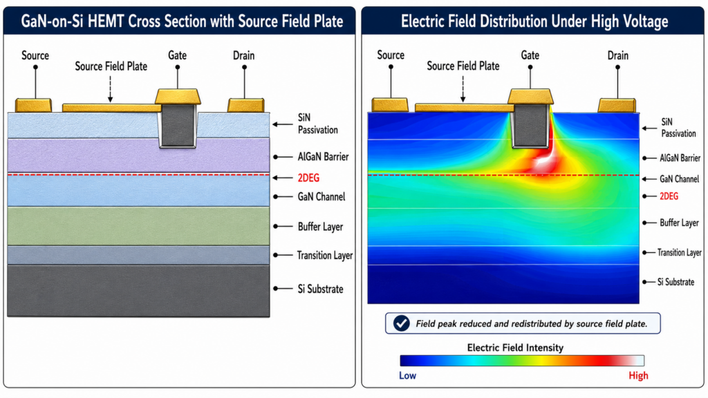
Pit Avoidance Guide (Veteran Field Experience): During high-voltage shutdown in hard-switching topologies, surface traps and epitaxial layer defects are extremely easy to capture electrons. If you drive the GaN power tube with a dV/dt as high as 200V/ns, the trapped electrons will not be released in time. As a result, the local 2DEG channel will narrow, causing catastrophic “dynamic Rdson drift” (also known as current collapse).
The way to break the situation: when selecting the model, resolutely abandon those tubes that are still designed with old passivation layers. Be sure to pick devices with advanced source field plate technology or p-GaN injection structures. They can reshape the electric field distribution and force the transient Rdson drift to less than 10%.
T.E.A. Evaluation Framework: SMPS And Inverter Selection Model
Engineers must abandon the isolated selection thinking of “headache” and honestly use the system-level T.E.A. (thermal, electromagnetic, architectural) matrix, so as to completely drain the limit switching capability of GaN HEMT on silicon.
Thermal Management (Thermal): Breaking the Lateral Thermal Bottleneck of Silicon Substrates
The lattice thermal conductivity of silicon (Si) is only about 1.5 W/cm · K, which is really a lot worse than silicon carbide (SiC). In those modules with limited volume and extremely high power density, the traditional bottom heat dissipation package will bring the junction temperature close to the dangerous red line of 150°C in minutes.
Experts suggest that if you want to make a totem pole bridgeless PFC design above 3kW, simply put the old TO-247 package and throw it into the garbage can. Directly on the top heat dissipation package such as TOLT, coupled with the direct pressure radiator, the thermal resistance can be reduced by at least 40%.
Electromagnetic (Electromagnetic): Deadly strangulation of parasitic inductance
Given the horrible switching speed of GaN HEMT technology, even a parasitic inductance of 1nH on the pin is enough to crash the whole system. Once the turn-on speed of 100V/ns hits the micron-level common source inductance (V = L * di/dt), violent ringing will be generated on the drive loop immediately, thus triggering a fatal through short circuit event.
PCB Layout Iron Law: The driver IC must be placed on the same layer of the PCB as the GaN tube, and the area of the driver circuit must be stuck within 5mm. Want to be stable? That must use Kelvin source (Kelvin Source) connection, the power circuit and drive circuit completely decoupled.
Architecture (Architectural): demanding drive voltage margin
The gate threshold voltage (Vth) of enhanced (e-mode) silicon-based GaN HEMT is generally very low, about 1.5V, and the absolute maximum rating rarely exceeds 6V.
Matching logic: If you want to directly apply the traditional Si MOSFET driver circuit, the tube will explode. The design must be dedicated wide band gap isolation driver IC, plus active Miller Clamp (Active Miller Clamp) circuit. In the bridge architecture, it is best to inject a negative bias of -2V to -3V on the shutdown path, which is the king to ensure absolute noise immunity.
Real Machine Duel: Silicon-Based Gallium Nitride VS Silicon Super Junction (SuperJunction)
To evaluate the silicon-based GaN power tube in switching applications, don’t pull the false, the hard core data in the laboratory is the only reliable touchstone.
Under the topology of 3.3kW high-frequency bidirectional DC-DC converter (300kHz switching frequency), we did a pressure comparison test with two devices with equivalent specifications:
Core Data Highlights:
Turn-off loss (Eoff):GaN is only 4.2 µJ, while Si is as high as 18 µJ.
Reverse recovery loss (Eoss):GaN is almost zero, but Si is surprisingly high (which directly limits its application in continuous conduction mode).
Peak efficiency of full-load system: GaN easily rushed to 98.7, while Si stuck at 96.2 due to the bottleneck of thermal runaway.
The measured data is ironclad: when the frequency soar above 300kHz, the silicon-based HEMT is currently the only cost-effective path to increase the system power density and completely eliminate the reverse recovery loss of the body diode.
Real Machine Duel: Silicon-Based Gallium Nitride VS Silicon Super Junction (SuperJunction)
To evaluate the silicon-based GaN power tube in switching applications, don’t pull the false, the hard core data in the laboratory is the only reliable touchstone.
Under the topology of 3.3kW high-frequency bidirectional DC-DC converter (300kHz switching frequency), we did a pressure comparison test with two devices with equivalent specifications:
| Performance Parameter | 650V GaN-on-Si HEMT | 650V Silicon SuperJunction (CoolMOS) |
| Gate Threshold Voltage (Vth) | ~1.5V (Very Low) | ~3.5V – 4.5V (Standard) |
| Absolute Max Gate Voltage | 6V (Stringent Margin) | ±20V to ±30V (Wide Margin) |
| Turn-off Loss (Eoff) | 4.2 µJ | 18.0 µJ |
| Reverse Recovery (Qrr / Eoss) | Nearly Zero | Extremely High |
| Peak System Efficiency (3.3kW @ 300kHz) | 98.7% | 96.2% (Limited by thermal runaway) |
| CCM Operation Suitability | Optimal | Severely Restricted |
| Turn-off Drive Requirement (Bridge Topology) | Dedicated driver with -2V to -3V negative bias & Active Miller Clamp | Standard 0V turn-off typically sufficient |
Core Data Highlights:
Turn-off loss (Eoff):GaN is only 4.2 µJ, while Si is as high as 18 µJ.
Reverse recovery loss (Eoss):GaN is almost zero, but Si is surprisingly high (which directly limits its application in continuous conduction mode).
Peak efficiency of full-load system: GaN easily rushed to 98.7, while Si stuck at 96.2 due to the bottleneck of thermal runaway.
The measured data is ironclad: when the frequency soar above 300kHz, the silicon-based HEMT is currently the only cost-effective path to increase the system power density and completely eliminate the reverse recovery loss of the body diode.
Frequently Asked Questions (Frequently Asked Questions)
Why do silicon-based GaN HEMTs use lateral structures instead of vertical structures?
Because of the lattice mismatch and the great difference in thermal expansion coefficient, it is physically impossible to grow a thick and defect-free drift layer on a silicon substrate. Today’s commercial devices cleverly bypass the bottleneck of “vertical penetration” and directly use the 2DEG on the surface of the heterojunction to let the current flow laterally.
For high-frequency switch design, should we choose enhanced (E-mode) or cascode (Cascode)GaN?
If you want to pursue the ultimate high-frequency performance and minimalist packaging, close your eyes and choose E-mode. Although it is demanding on the accuracy of the gate drive, the win is that the reverse recovery is completely zero. Cascode, the normally off state is realized by 1 a low-voltage Si MOSFET in series, which has the advantage of being compatible with the old silicon driver. However, the price is the introduction of Coss of silicon tube and a trace amount of Qrr. Once the frequency exceeds 1MHz, this thing will seriously drag its feet.
What is the difference between the avalanche breakdown capability of GaN power transistors and Si MOSFETs?
Silicon MOSFETs rely on the depletion layer of the physical PN junction to absorb the transient avalanche energy. However, the lateral GaN HEMT does not have a traditional PN junction at all, so it does not have a standard avalanche rating. The secret of its life-saving response to overvoltage surges is its great transient voltage margin (a nominal 650V tube usually carries a dynamic breakdown of 900V to 1200V).
In hard-switching GaN-on-silicon applications, how should engineers handle high-frequency EMI problems?
Very high dv/dt will naturally explode a serious high frequency common mode noise. To deliberately lower the switching speed in order to reduce noise? That is a faint move at the expense of efficiency. The core solution is to compress the area of the high-frequency parasitic loop, set a high-frequency ferrite bead on the gate drive resistor to suppress the UHF ringing, and finally put on a control IC with a spread frequency (Spread Spectrum) function to smooth the EMI spectrum profile.
How does p-GaN gate technology improve the reliability of GaN HEMT on silicon?
The native 2DEG channel is Normally-on. The clever thing about p-GaN gate technology is that it injects a hole-rich p-type GaN cap layer directly above the gate region, which abruptly pulls up the conduction band energy level, thus depleting the electron gas below. This not only achieves an extremely reliable normally-off (Normally-off) characteristic, but also greatly broadens the forward gate voltage margin, greatly reducing the risk of misdirection.