 Neditek
GaN Vs GaAs Power Amplifier: Choosing For RF Designs
The material inside an RF power amplifier matters, but it cannot select the amplifier for you. A transmitter that needs substantial output power has a different problem from a compact gain stage that must fit a tight power and board budget. In a gan vs gaas power amplifier comparison, start with the signal, operating conditions, and required output at the system interface. Then see which device meets those conditions with a workable bias and thermal design.

Where The Technologies Tend To Fit
GaN is attractive when an RF output stage needs high power density. Its high breakdown field and current density support high-power RF designs, while GaN-on-SiC is commonly used where heat must spread away from a dense microwave device. These material advantages are useful design options, not a guarantee that every GaN amplifier delivers better efficiency or bandwidth in a finished circuit.
GaAs remains useful in lower-power amplification, driver stages, low-noise functions, and mature MMIC implementations. A GaAs part may be the more practical choice when its gain, package, supply voltage, and output capability already satisfy the link budget. Both technologies can appear in one transmit chain: a GaAs gain stage can drive a higher-power GaN output stage, provided the interface power, impedance, bias, and thermal coupling are checked.
Make The Power Numbers Comparable
The first trap is comparing unlike specifications. Saturated output power, or Psat, describes a different operating point from P1dB, the output at 1 dB gain compression. Neither automatically states the usable average output with a modulated signal. For a linear transmitter, the required back-off, adjacent-channel performance, error vector magnitude, and efficiency at the actual average power matter as much as the headline power figure.
Neditek's catalog illustrates why the labels deserve attention. Its GaN amplifier NDGB010008 is listed for 3.4 to 3.6 GHz with a 56.3 dBm Psat and 48 V drain voltage. The listed LTE efficiency is 42% at 48.0 dBm, a specific operating point rather than an efficiency claim at Psat. GaAs amplifier NDGB020005 covers 3.3 to 3.8 GHz and lists 2 W output, 33.5 dBm P1dB, 34 dB gain, and a 5 V supply. The bands overlap, but the power definitions and intended power levels differ. Comparing 56.3 dBm Psat directly with 33.5 dBm P1dB would obscure the actual design question.
Check Gain, Linearity, And Efficiency Together
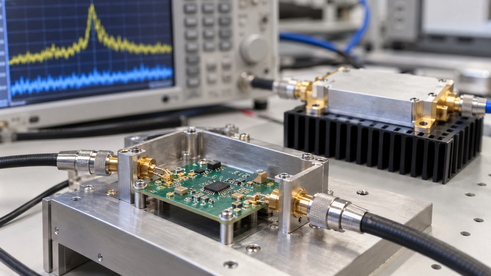
An amplifier with higher output power may need more drive or a different driver chain. Work backward from the required antenna or connector power, accounting for filters, switches, cables, and any power combining losses. Confirm that the preceding stage can deliver the input power without losing its own linearity margin.
For a modulated communication waveform, ask for gain, efficiency, and linearity under the same waveform, bandwidth, output level, bias, and temperature. A large-signal efficiency number measured near saturation does not describe operation at backed-off average power. For a pulsed radar application, peak output, pulse width, duty cycle, phase behavior, and cooling conditions become central instead. The right comparison uses the waveform the amplifier will actually see.
Frequency And Package Change The Result
Do not treat a material name as a frequency specification. A device can be capable of operation across a stated range while its reference matching circuit works only over a narrower band. Review gain and power across the full required band, especially at its edges. Check whether the quoted result is measured at the package pins, a demonstration board, or a later system connector.
Package and board layout affect both RF loss and heat flow. A compact GaAs QFN device and a high-power GaN package impose different mounting, grounding, and cooling tasks. If the GaN device is chosen for power density, the thermal path through die attach, package, interface material, and heat sink still has to support the intended continuous or pulsed duty. A favorable substrate property alone cannot establish the final channel temperature.
A Practical Selection Sequence
Define the frequency limits, waveform, required average or peak output, linearity target, ambient temperature, and available cooling. Set the supply and mechanical constraints next. For each candidate, compare the same power metric at the same reference plane, then examine gain, efficiency, and linearity at the required operating point. Finally, validate the complete bias, matching, and thermal arrangement on a representative board.
The resulting choice may be GaN for a demanding high-power output stage, GaAs for a compact lower-power gain stage, or a combination of both. In each case, a part-level data sheet and application-specific measurements give a more reliable answer than a broad material ranking.