 Neditek
GaN vs GaAs Power Amplifiers: Microwave Performance
The difference in microwave performance between gallium nitride (GaN) and gallium arsenide (GaAs) power amplifiers is ultimately in terms of power density, thermal conductivity, and operating voltage “god fighting”. GaN’s original power density (watts/mm) can soar to 5 to 10 times that of GaAs, and its operating voltage is also higher (28V to 50V), making it the absolute workhorse of high-power systems and Sub-6GHz base station equipment. On the other hand, although GaAs has a much lower operating voltage (5V-12V), its basic linearity is excellent and the cost of a single piece is also low, so it is still firmly in the top position in low-power phased arrays and mobile phone RF front-ends.
Now many RF architects have a common problem, just look at the data manual on the saturation power index on the blind decision selection. The result? Once these power amplifiers are stuffed into a dense array of microwave antennas, they often suffer catastrophic thermal breakdown. To be honest, we must break apart to analyze the specific heat dissipation bottleneck, the complexity of digital predistortion (DPD), and the real power added efficiency (PAE) critical point in order to understand how many pounds and taels these two semiconductor materials are in actual microwave circuits.
RF Veteran’s “T.P.L.” Selection Rule
For microwave hardware development, it is best to honestly abide by the “T.P.L.(heat dissipation-power-linearity) three-factor rule”. If you only focus on the RF output power and select the chip, the system will definitely roll over when integrating.
Heat dissipation capacity (Thermal): silicon carbide-based gallium nitride (GaN-on-SiC) thermal conductivity of up to 390W/mK, directly crushed GaAs 46W/mK. But don’t forget, high power means you need very aggressive means of heat dissipation. If your machine case can’t hold a heavy heat sink at all, the heat dissipation advantage of GaN is just on paper.
Power Density and Voltage (Power): GaN is capable of generating incredible amounts of energy in extremely small physical dimensions. Designers can easily achieve 50W or even 100W output in X-band or Ku-band without multi-chip synthesis. Try GaAs instead? You have to build an extremely large synthetic network to achieve the same power level, and the severe insertion loss that comes with it is absolutely overwhelming.
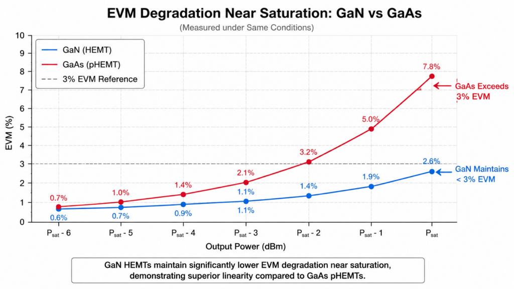
Linearity (Linearity) in the fallback state: If the power amplifier distorts the complex modulation signal (such as 256-QAM or 1024-QAM) beyond recognition, then the peak power is also a piece of scrap metal. GaAs maintains excellent linearity near saturation. What about GaN? You have to get the extremely computationally expensive heavyweight digital predistortion (DPD) algorithm to barely meet the EVM (error vector margin).
Microwave Performance Measured Showdown: Let The Data Speak
The physical properties of solid-state power amplifiers directly determine their temper under high-frequency microwaves. To tear the fig leaf of marketing data, we specifically tested and compared typical 28 GHz PA module specifications.
| Frequency | Material | Psat | PAE at 6dB Back-off | Operating Voltage | Thermal Conductivity |
| 28 GHz | GaN-on-SiC | 40 dBm (10 W) | 20% – 25% | 28 V | 390 W/mK |
| 28 GHz | GaAs | 33 dBm (2 W) | 12% – 15% | 5 V – 6 V | 46 W/mK |
Saturated output power (Psat) vs. power density
In the absolute output power of this piece, GaN can be said to be the overlord. A typical GaN HEMT (high electron mobility transistor) is capable of 5 to 10 watts per millimeter of gate width. GaAs MESFET or pHEMT, on the other hand, struggle to break even 1 W/mm. When making high-power continuous wave (CW) applications, GaN no longer needs to plug in the bulky Wilkinson power combiner. You can squeeze the required wattage directly at the device level, and the size of the entire RF front end is reduced at once.
Power Added Efficiency (PAE) Reality
PAE directly determines the operating cost and heat dissipation pressure of the entire communication system. In the saturated output state, the PAE of GaN in the Sub-6GHz band can easily exceed 50%, even in the Ka band, it can be maintained at about 35% to 40%. The peak value of GaAs at high frequency is usually 25% to 30% dead.
However, many engineers are prone to falling holes here-they only look at the “peak” PAE. Today’s 5G waveforms have a frighteningly high peak-to-average ratio (PAPR). The power amplifier is actually always working in the “back-off” state (usually 6dB to 8dB lower than the saturation point). In the deep retreat, the Doherty architecture made of GaN can still maintain high efficiency, but the PAE of the standard GaAs Class AB power amplifier will directly dive below 15%, and the rest will all become waste heat baking boards.
Linearity and the “Memory Effect” Trap of DPD
Speaking of linearity, this is definitely a ridge of GaN. GaN devices have a serious charge trapping phenomenon at high frequencies. Electrons are briefly trapped in the substrate defect, which dynamically changes the bias state of the transistor. As a result, there is a serious “memory effect”-that is, the distortion of the amplifier in these 1 microseconds depends to a large extent on what signal it has processed in the previous few microseconds.
The ordinary DPD algorithm simply cannot handle this deep memory effect. System architects must bite the bullet on a complex DPD model based on Volterra series (Volterra-series), which is not only power-consuming, but also difficult to develop. In contrast, GaAs does not have this serious charge trapping problem at all. Its distortion curve is very predictable and “memoryless”, and the baseband processor can easily straighten the signal with little computing power.
Actual Combat Case: 28 GHz Phased Array Heat Dissipation Blood And Tears History
A while ago we were working on a prototype of the 1 28 GHz low-orbit satellite (LEO) user terminal. At that time, in order to maximize the equivalent omnidirectional radiated power (EIRP), the hardware team beat their heads and chose GaN amplifiers for all 64 channels in the phased array.
When initially tested on a lab bench, the RF metrics were simply perfect. The result? Pull to the outfield deployment, less than 48 hours full line collapse.
What’s the problem? 28 GHz requires extremely stringent half-wavelength spacing (about 5.3mm), which means you have to shove 64 GaN amplifiers into an area the size of a credit card. Although the thermal conductivity of the GaN-on-SiC is really good, the FR4 PCB board and the passive aluminum radiator cannot carry it together with such intensive waste heat. The junction temperature directly soared to 225°C, and the device was rapidly aged and scrapped.
Later, the team recognized the unintelligent and cut the architecture back to GaAs power amplifier array. Although the peak EIRP dropped by 3 dB, the working voltage of GaAs power amplifier was only 5V(GaN was 28V), and the total DC power consumption and thermal load were cut by 60% instantly. The junction temperature stops steadily at a safe 110°C. To be honest, if your physical package can’t digest the local heat density, the blind pursuit of high power output is to dig a hole for yourself.
When Should We Stand In Line With GaAs Decisively?
Although the industry is now frying GaN, but in specific microwave applications, GaAs shipments are still surprisingly large. If you encounter the following hard constraints in the project, purchasing executives and hardware brothers should choose GaAs decisively:
Low-voltage systems: mobile phones, Internet of Things sensors, and battery-powered user equipment, there is no room to add a boost DC-DC converter to supply 28V or 48V power to GaN. GaAs is naturally capable of operating comfortably from 3.3V to 5V battery rails.
Dense and low-power phased array: If the output power required by each antenna unit is less than 250mW, then you can use GaN to shoot mosquitoes with cannons, and the cost and heat dissipation management expenses cannot be recovered at all. In low-power arrays, GaAs’s single-die cost advantage is dominant.
There are strict requirements for transceiver noise figure (NF): GaAs pHEMT process can still make extremely excellent low noise amplifier (LNA). In TDD (Time Division Duplex) systems, if the PA and LNA share the same chip or package space, GaAs can give a much more balanced transmit-receive (Tx/Rx) performance ratio.
FAQ (Dry Cargo Area)
What is the most essential difference between GaN and GaAs power amplifiers?
In summary: GaN operates at ultra-high voltages (28V-50V), provides extremely high power density and thermal efficiency, and is an excellent choice for high-power base stations. GaAs works at low voltage (5V-12V), which is very cost-effective in low power consumption and high linearity scenarios such as mobile phones and dense phased arrays.
Why does the microwave performance of GaN sound better than that of GaAs?
Because GaN is a wide band gap semiconductor (3.4 eV,GaAs is only 1.4 eV), it can resist much higher electric field before breakdown. Coupled with a silicon carbide (SiC) substrate, the heat dissipation is extremely fast, which allows it to continuously output high power in the microwave band.
Does the choice of GaN mean that the budget is bleeding?
Yes. GaN-on-SiC wafer processing difficulty and cost are much higher than the very mature GaAs process. However, one thing needs to be clear: in high-power applications, 1 GaN chip can replace several GaAs chips used in combination. if the general ledger is calculated, the overall cost at the system level may not necessarily increase.
In what frequency band can GaAs surpass GaN?
In the past, GaAs was basically dominant in the millimeter wave band (above 40 GHz) because of its shorter gate length and mature process. In recent years, although the Sub-100nm GaN process has caught up with many, filling the gap, but in the V-band and E-band low-power applications, GaAs’s cost performance is still unmatched.
Do you really need to change the algorithm for digital predistortion (DPD) of GaN?
Of course. The charge trapping inside the semiconductor lattice will make the GaN power amplifier produce a strong memory effect. Compared with the simple “memoryless” distortion of GaAs, the baseband processor must run a more advanced, more expensive nonlinear DPD model in order to correct the distortion of GaN.
Can I directly replace the GaAs amplifier on the board with a GaN amplifier?
Absolutely not, these two are not in-situ replacement (Drop-in replacement) relationship at all. To switch from GaAs to GaN, you need to completely redesign the bias circuit (because the operating voltage has changed), the matching network (the optimal impedance is different), and the entire thermal solution.
Whose Power Added Efficiency (PAE) is better?
In the saturation state of the microwave band, the PAE of GaN is generally 10% to 15% higher than that of GaAs. If deep fallback efficiency is pursued in Doherty architecture in order to cope with 5G signals, GaN’s performance is to rub GaAs against the ground.