 Neditek
How Does A Low Noise Amplifier Work Without Losing Gain?
The reason why low-noise amplifiers (LNAs) can operate without losing gain relies on inductive source generation (LNA) technology. It can pull the optimal noise impedance (Gamma Opt) extremely close to the complex conjugate of the input impedance. This method not only prevents thermal noise from being amplified, but also strictly preserves the signal strength at the front end of the receiver. Well, that’s the standard answer in textbooks. But based on my experience coaching hardware teams, to play around with this on a real PCB while maintaining the gains of LNA, you need to be extremely precise in your management of parasitic parameters and active bias. Next, let’s directly disassemble how to achieve full gain while suppressing noise in engineering.
Uncovering The Core Logic: How Do Low-Noise Amplifiers Work?
The role of LNA is to receive and amplify radio frequency signals at the microvolt level from the antenna while minimizing the thermal noise generated internally. Ordinary amplifiers are rough and usually amplify the signal and background noise together, which directly destroys the signal-to-noise ratio (SNR). LNA needs to amplify the main signal independently before the mixer at the back messes up the signal further. This actually follows the Friis transmission equation ——the system noise is absolutely determined by the first level.
Fatal Flaw In Standard Conjugate Matching
When reviewing images, I often find that many engineers work hard on standard conjugate matching from the beginning, and as a result, the performance of LNA is directly ruined. Simply performing input impedance matching (conjugate matching) for maximum power transmission will often force the amplifier to an operating point that deviates greatly from the minimum noise figure. On a Smith chart (Smith Chart), the best noise matching point and the best gain matching point are exactly on two different impedance coordinates. Hard-hitting one of them will definitely destroy the other.
Inductive Source Extreme Negative Feedback (Real Solution)
At this time, the negative feedback of the inductive source is the positive solution, which directly resolves the mathematical conflict between gain and noise. A precisely calculated inductance is inserted between the emitter (or source) of the active transistor and ground, which can change the real part of the input impedance without introducing thermal noise. This inductor on the Smith chart is really bringing the best gain point and the best noise point closer together. This way you achieve simultaneous noise and input matching (SNIM).
“GNI Balance Matrix ” Model
After I disabled hundreds of substandard RF front-ends in the lab a few years ago, I came up with a set of GNI ( gain-noise-impedance) balance matrix. To be honest, it is impossible to fill all three variables at the same time. You have to dynamically optimize this matrix based on the specific sensitivity metric of your current receiver.
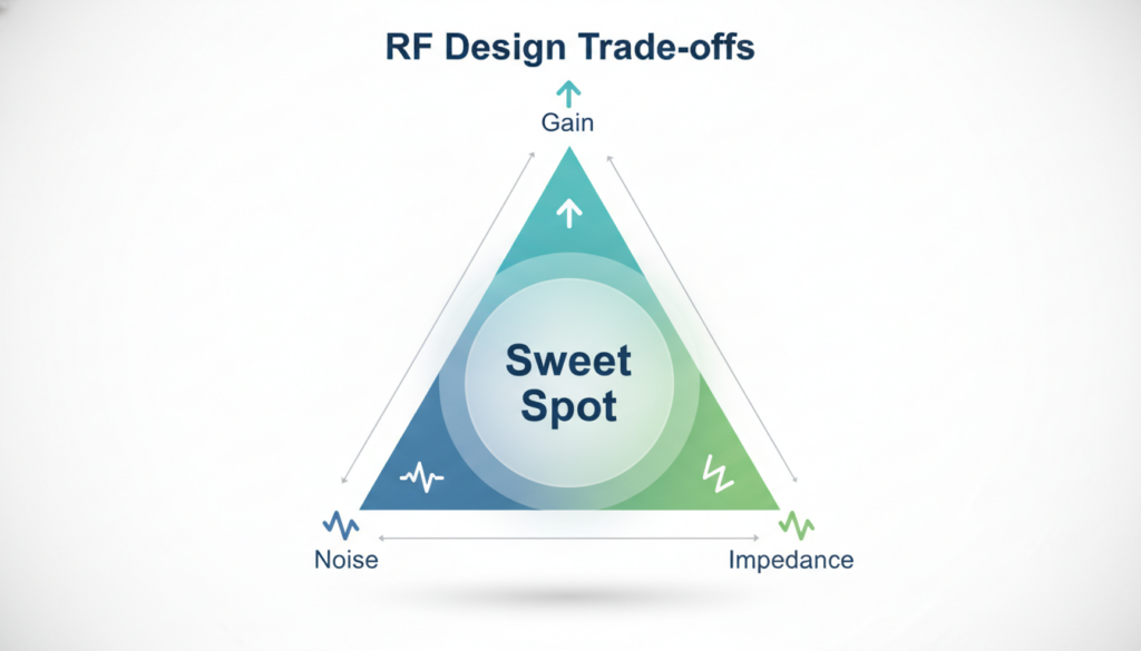
Vector 1: Gain (S21) Optimization
The gain of the LNA depends strongly on the transconductance of the core transistor. Increase the bias current, lift the transconductance, and your S21 indicator will naturally look better. But if you push the bias current too hard, you introduce shot noise, which directly raises the overall noise figure (NF).
Vector 2: Noise Factor (NF) Minimization
Choosing the right transistor geometry basically sets your base noise floor. Large transistors have low base resistance (which reduces thermal noise), but they introduce high parasitic capacitance. This capacitor reaches the high frequency stage and eats the gain very hard. The transistor must be sized to fit right on the point where it matches your operating frequency band.
Vector 3: Impedance (Zin) Convergence
Components with high Q values (quality factors) must be on the input matching network. If you use a low-Q inductor at the LNA input, its built-in resistive loss is sufficient. Before the first active device, for every additional 0.1 dB of insertion loss, the system noise figure was firmly added with 0.1 dB, and the theoretical gains you ran out in the EDA software were immediately smoothed out.
3 Hidden PCB Layout Traps That Ruined LNA Gain
No matter how beautiful the theoretical circuit drawing is, the real FR4 or Rogers board will often be revealed in its original form. The parasitic parameters brought in by the physical traces are completely invisible on the schematic.
Trap 1: Parasitic Inductance of Grounded Vias
In the microwave band, a grounded tap is actually an inductance you don’t want at all. A single ground tap can add about 0.5nH of inductance to your source negative feedback path. This extra parasitic inductance will completely deflect the resonant frequency, causing the LNA to have extremely high noise and loss of gain in the target frequency band. My usual solution is to directly drill multiple parallel holes as close to the transistor ground pin as possible to reduce the parasitic inductance proportionally.
Trap 2: Input trace microstrip loss before IC
If the trace between the antenna switch and the LNA input is too long, it becomes a natural attenuator. The roughness and dielectric loss factor (Df) of the copper foil surface will swallow up the already weak signal little by little. The input trace must be shortened with extreme restraint. It is best to use a coplanar waveguide (CPWG) structure with a stitched ground hole to lock the electromagnetic field and preserve the signal integrity.
Exclusive Real-World Example: Recovering The 2.4dB Gain Lost In A 5.8GHz Receiver
Last month, I led a team to bug a 5.8 GHz IoT receiver when it was experiencing severe coverage distance issues. The original EDA simulation ran out with a gain of 16dB and an NF of 1.2dB. As a result, the physical prototype only had a gain of 13.6dB when it was shot, and the NF soared to 2.1dB.
We skipped the regular error scheduling process and took the bare board to the upper domain reflectometer (TDR) and scanned it. As soon as the data came out, at that position on the LNA input pad, the impedance dropped directly to 38 ohms. After investigation, it was found that the PCB board factory had enlarged the window of the solder mask layer, changed the local dielectric constant, and rigidly created a capacitive stub.
Later we cut the width of the input pad by 4 mils to compensate for the capacitance, and then changed the input matching capacitance to a high-Q winding type. The results are clear: the gain returns to 15.8dB and NF stabilizes at 1.25dB. Device selection and pad geometry can really directly determine your final performance limit.
Cutting-Edge Materials: GaN-On-SiC Is Pushing The Gain Limit
In the LNA market of Sub-6GHz in the past few years, silicon germanium (SiGe) and CMOS have basically dominated. But I’ve recently had a clear feeling that GaN-on-SiC (silicon carbide-based gallium nitride) is reshaping the design logic of the entire receiver. GaN has ridiculously high electron mobility and breakdown voltage. This allows our hardware engineers to design LNAs without having to hang a protective limit switch in front of the amplifier even if the input blocking signal is hard-resistant to +20 dBm. Just remove that limiter switch and you can save 0.5dB of input loss in an instant, and the system noise figure and effective gain will win directly.
Frequently Asked Questions (FAQs)
Why does increasing the bias current in LNA sometimes cause the gain to drop?
Because you push the bias current too hard, the transistor is squeezed out of the optimal active region and falls directly into the saturation region. At this time, the transconductance curve is flat. No matter how much current you add, it will not amplify the signal. Instead, it will generate excess heat and thermal noise, which will directly pull down the signal quality.
What exactly is the difference between LNA and ordinary RF amplifier?
The core mission of LNA is to suppress the noise figure (NF) while amplifying the signal at the front end of the receiver. Ordinary RF amplifiers (such as power amplifiers PA) are usually placed at the transmitter. They only focus on maximizing output power and efficiency and basically do not care about how much noise is generated internally.
How does source-pole negative feedback improve LNA stability?
Inductive source-pole negative feedback is equivalent to adding a negative feedback to the circuit. Transistors are most likely to oscillate at low frequencies, and this negative feedback is just enough to suppress the low-frequency gain, forcing the Rollett stability factor (K) above 1 without introducing any additional thermal noise into the main RF path.
Can I do LNA input matching with a normal 0402 inductor?
The ordinary 0402 multilayer inductance has a very low quality factor (Q), which is equivalent to introducing a series resistor. This resistor acts as a back attenuator before the signal even enters the amplifier. At the input level, in order to prevent the noise coefficient from deteriorating, it is honest and practical to use a wound high-Q inductance.
Why are Friis transport equations so deadly for LNA design?
Because the Friis equation mathematically sentences you to death: the noise figure of the entire receiving link, overwhelmingly depends on the first-stage equipment. If your LNA itself has a high noise figure, or insufficient gain, the noise generated by the mixer and filter that follows will directly bury your target signal forever.
3. Next Generation Low Noise Amplifier Frontier Applications
3.1 quantum computing read link
The signal power output by the superconducting qubit is ridiculously weak (-130 dBm or less). The LNA application scenario here is at the 4K level of the dilution refrigerator. In order to withstand the huge I/O scale required to 1000 multi-qubit systems, engineers are moving from discrete HEMT modules to fully integrated SiGe BiCMOS arrays.
3.2 Sub-THz 6G Massive MIMO
Once the frequency band is pulled up to between 100 GHz and 300 GHz, the traditional CMOS miniature law completely fails due to the low ft/fmax ratio. The application of 6G low noise amplifier began to rely on heterogeneous integration, directly bonding the D-band InP or GaN LNA to the silicon-based beamforming chip. The gain deviation between multi-channel arrays must be controlled within 0.5dB to prevent spatial beam distortion.
3.3 Automotive 77GHz FMCW Radar
Autonomous driving (including heavy AGVs in smart factories) has changed the requirements for radar, and the interference environment has become extremely dense. The selection priority has shifted from the original noise figure to extreme linearity (IIP3 > 0 dBm). Radar front-end now uses a large number of high-linearity cascode structure, with active interference cancellation loop, to prevent being blocked by the radar transmission signal of adjacent vehicles.
4. Expert Pit Avoidance Guide: Simulation Software Didn’t Tell You The Truth About Millimeter Wave Packaging
Many people tend to rush to sign a stream just by looking at the schematic or the noise figure run out by the rough layout parasitic parameter extraction (RCX), which is an extremely deadly trap.
Share 1 set of real laboratory data: In a recent 28GHz 5G front-end project, the inductively degraded LNA ran out of an extremely ideal 1.4dB noise figure in simulation. Results After the assembly (using standard QFN package), the measured NF directly deteriorated to 2.9dB.
The root cause of the investigation is the inductance of the ground bond wire. Even 0.1 nH of unmodeled parasitic inductance in the ground loop creates an unexpected series feedback loop out of thin air in the 28GHz band. This particular feedback completely changes the real part of the optimal noise impedance (Zopt), pulling it completely away from the 50 ohm conjugate match point.
Complete solution: full 3D EM co-simulation must be performed, taking into account all the specific PCB stacks, solder bumps and ground pads of the package. As long as the frequency is over 15GHz, it is directly switched to flip chip (C4) package, and the parasitic inductance is dead at the picheng (picohenry) level.
5. Frequently Asked Questions (PAA)
How do you decide whether to use CMOS or GaN in an LNA design?
Considering its survivability against high input power, GaN has the advantage of rolling (continuous wave up to 5W without limiters), which makes it a must for macro base stations. With low-cost and high-density logic integration capabilities, CMOS dominates highly integrated, low-power mobile terminals and IoT devices.
What is the effect of the Miller effect on the LNA topology?
The Miller effect multiplies the gate-drain parasitic capacitance (Cgd) by a multiple of the amplifier’s voltage gain. This can cause a catastrophic surge in total input capacitance, disrupting impedance matching in the high band. This is the main reason why the cascode (Cascode) topology is widely used to neutralize this effect.
Can LNA achieve a noise figure of less than 1dB at room temperature?
Yes. For specific narrow frequency bands (such as L-band satellite receivers), specially customized discrete GaAs pHEMT or advanced InP transistors can normally achieve a noise figure of 0.3dB to 0.8dB at room temperature.
Why does increasing the bias current not always reduce the noise figure?
The transistor noise is composed of a combination of thermal noise and induced gate noise. Although pulling up the current density (gm) initially reduces the channel thermal noise, this eventually increases the induced gate noise and reduces the optimal source resistance, causing the minimum noise figure (NFmin) to rise instead.
What is the difference between Noise Match and Power Match?
Power matching (conjugate matching) aims to maximize signal transmission, while noise matching optimizes the source impedance (Zopt) presented to the transistor to minimize the internal noise contribution. In broadband designs, these two impedances rarely overlap, which requires specific topologies such as noise cancellation or inductive degeneration to bridge the gap.
How does the LNA handle out-of-band interference?
Without a high IIP3, strong out-of-band signals can push the LNA into the compression region, causing the receiver to desensitize (block), or produce intermodulation distortion (IMD) that falls within the desired frequency band. Conventional practice is to place a SAW/BAW filter at the front end of the LNA to reject these signals.
Why are distributed amplifiers rarely used in consumer 5G phones?
Distributed amplifiers consume extremely high DC power, and the required on-chip transmission lines consume a large amount of silicon area due to their long physical length. For mobile devices, battery life and compact size are a much higher priority than the flat gain of multi-octave.