 Neditek
Power Amplifier vs Low Noise Amplifier: 5 Core Differences
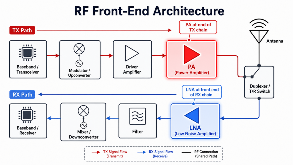
What is the difference between a power amplifier (PA) and a low noise amplifier (LNA)? The most fundamental difference lies in their position in the system architecture and their respective core optimization goals. The PA is kept at the end of the transmit end (TX), spells out the output power and efficiency (PAE), and abruptly pushes the signal to the antenna. The LNA stands at the entrance of the receiving end (RX). Its unique skill is to amplify the weak signal at the microvolt level and at the same time press the thermal noise (that is, Noise Figure) generated by itself to an absolute minimum.
Understanding these basic concepts is just getting started. Many hardware veterans stumbled when doing radio frequency certification, not because they did not understand the concept, but because they weighed the wrong indicators-for example, they sacrificed the linearity of LNA in order to gather gain, or failed to improve the load impedance of PA. Next, let’s break up these specific parameters, selection ideas and easy-to-step pits in engineering to help you thoroughly complete the RF front-end design.
The original S.P.L. I .T. rule of assessment
Senior engineers often use the S.P.L. I .T. rule when distinguishing and evaluating PA and LNA. You can use this model to align your purchasing needs and design specifications:
S-signal processing (Signal Handling): PA deals with pre-processed signals with high energy; LNA is “looking for a needle in a haystack” in the background noise to restore signals that have been attenuated and full of uncertainty.
P-position (Placement): PA is the last gate before the signal enters the transmitting antenna; LNA is the first gate after the signal leaves the receiving antenna.
L-linearity focus (Linearity Focus): PA linearity (OIP3) determines how serious out-of-band leakage (ACLR) is; LNA linearity (IIP3) determines its anti-interference and anti-blocking capabilities.
I-impedance strategy (Impedance Strategy): the output of the PA is matched in order to pursue maximum power transfer; the input of the LNA is matched in order to pursue minimum noise.
T-heat dissipation limitation (Thermal Constraints): PA is a large heat generator and relies heavily on heat dissipation design (such as heat sink and via hole); Although LNA does not generate much heat, it is extremely sensitive to changes in thermal noise.
| eature | Power Amplifier (PA) | Low Noise Amplifier (LNA) |
| Primary KPI | PAE / Output Power | Noise Figure / Gain |
| [S] Signal Handling | Massive, pre-conditioned signals | Degraded, unpredictable signals |
| [P] Placement | Last active stage (Before Tx antenna) | First active stage (After Rx antenna) |
| [L] Linearity Focus | OIP3 (Dictates ACLR / out-of-band emissions) | IIP3 (Dictates resistance to blocking / jamming) |
| [I] Impedance Strategy | Output matching ➔ Maximum Power Transfer | Input matching ➔ Minimum Noise |
| [T] Thermal Constraints | Heavy Dissipation (Requires heatsinks / vias) | Cool Operation (Highly sensitive to thermal noise) |
5 core differences between PA and LNA
1. The Chain Reaction Of Architectural Location And Link Budget.
The PA is the end of the transmit link and the LNA is the beginning of the receive link. The PA receives the modulated RF signal from the transceiver, pulls the amplitude up to the upper limit required by regulations (such as 30 dBm), and then feeds it to the antenna. In turn, the LNA is responsible for capturing the weakly attenuated signal caught by the receiving antenna (usually as low as -100 dBm) and amplifying it to the level that the subsequent mixer can handle.
According to the Friis formula, adding even a little loss in front of the LNA will degrade the noise figure of the entire system one to one (dB to dB). Therefore, if a filter is added in front of the LNA, the price is to sacrifice the critical receiving sensitivity. For PA, the insertion loss after the output will only force PA to push with greater strength, resulting in more power consumption and more serious heat generation.
2. Core KPI Showdown: Efficiency Vs. Noise Figure
Picking PA mainly depends on power added efficiency (PAE) and 1dB compression point (P1dB), while the standard for judging LNA is often noise figure (NF).
The task of the PA is to convert direct current into radio frequency power. High PAE means power saving and not easy to reduce frequency, which is a life-saving indicator for mobile phones and high-density base stations. P1dB circles the limit power that the PA can output before the signal is distorted.
LNA, on the other hand, focuses almost entirely on NF. Even in the top-of-the-line amplifiers, the internal electronic scurry produces thermal noise. An NF achieves an LNA of 0.8 dB, which hardly introduces additional noise when amplifying weak signals, which preserves the signal-to-noise ratio (SNR) necessary for high-order modulation (such as 256-QAM).
3. Input Signal Range And Dynamic Constraints
The input signal that the PA faces is usually from the baseband processor, and the amplitude is high and controllable; but the LNA 1 is born to face an extremely chaotic and unknown reality environment.
The input drive level of the PA is usually very stable, probably between -10 dBm and 0 dBm. PA is designed to work in the saturation zone or near the saturation point in order to squeeze it out for maximum efficiency.
The LNA operating environment is much more dynamic. It must be sensitive enough to capture a weak signal of -110 dBm, but also enough to “beat”-when a nearby interference source or transmitter suddenly hits a strong signal of -20 dBm, it cannot collapse directly. This resistance is measured by the input third-order interchange intercept point (IIP3) in the industry.
4. Semiconductor Technology And Chip Materials
The physical characteristics of the transistor largely determine the division between the two brothers.
Today’s PAs rely primarily on gallium nitride (GaN) or gallium arsenide (GaAs). GaN is simply invincible in breakdown voltage and thermal conductivity, so it is logical to become the first choice for 5G macro base stations and high-power radars.
In the past, LNA preferred GaAs pHEMT process, but in recent years, the wind has changed, and silicon germanium (SiGe) and silicon on insulator (SOI) have become popular. SOI process enables LNA and RF switch to be integrated on the same wafer very cheaply, which not only makes the boards of smart phones and IoT modules very small, but also can stabilize the noise figure below 1dB.
5. The Underlying Logic Of Impedance Matching
Simply put: engineers match the PA to “rough” transfer energy, and the LNA to “cheat” physics.
For both devices, the standard 50 ohm match is rarely optimal. Matching PA output usually depends on the measured data of “Load Pull”. The impedance point you are looking for is the most perfect compromise between output power and PAE.
The input of the LNA requires “Gamma Opt”. The impedance point that allows you to get the maximum gain is definitely not the point with the lowest noise. Therefore, RF engineers will deliberately “mismatch” (discard part of the energy transmission efficiency) at the LNA input to abruptly remove the absolute lowest noise figure curve.
Hardware engineers must see the pit guide
What is written in the data manual is always the ideal state in the laboratory, but 1 to the reality, the rest is often eaten clean. According to our extensive field failure analysis, the hardware team must avoid the following dead holes:
LNA trace loss trap: If the PCB trace from the antenna to the LNA input is pulled very long, it is definitely a fatal mistake. Even if there is only 1 dB insertion loss on the FR4 line in front of the LNA, the noise figure of the entire system will directly soar by 1 dB. Remember, within the scope of the layout, the LNA attached to the antenna feed point as close as possible.
PA standing wave ratio (VSWR) burn: there is no perfectly matched antenna in the world. If the antenna is detuned (for example, the user’s hand just holds the antenna part of the mobile phone), the standing wave ratio (VSWR) will instantly rise. RF energy is ejected back to the PA. If there is no isolator, or if the VSWR mismatch resistance of the PA itself is not strong (usually it is required to withstand a 10:1 mismatch), the PA will thermally run out of control and eventually be permanently scrapped.
PA leakage causes LNA “blinding”: In TDD (time division duplex) systems, if the isolation of the RF switch is too poor, a 1 small part of the energy output by the PA will leak into the input of the LNA. Don’t underestimate this short moment, even if only 15 dBm leakage, but also enough to break down the fragile LNA gate oxide. Be sure to do adequate isolation, or simply choose an LNA with internal bypass (Bypass) protection mode.
Frequently Asked Questions (FAQ)
What If I Use The LNA As A PA?
In a word: it will be saturated in seconds, the signal will be seriously distorted, and then the high probability of direct burning. LNA’s P1dB compression point is extremely low, and its foundation simply cannot withstand the huge current required to drive the antenna, nor can it dissipate that heat.
Can You Use PA As LNA?
Technically it does amplify the signal, but it can ruin your receiver. The noise figure of the PA is very high (usually 5 dB to 8 dB or even more exaggerated). If the PA is placed at the receiving end, the weak signal will be directly submerged by the PA’s own huge bottom noise, and the budget of the entire link will be completely destroyed.
What Is The Impact Of GaN (Gallium Nitride) Technology On PA And LNA?
Because of its wide band gap characteristics, GaN is extremely rough to improve the power density and efficiency of PA. Although GaN is usually exclusive to PA, there are now some low-power GaN processes that are beginning to be used in the receiving front end. The advantage of this front end is that it can survive extreme blocking signals even without limiter protection.
Is The Cost Difference Between PA And LNA Large?
PA is usually more expensive. Because it needs to handle large currents, the chip area is large, the heat dissipation package is complicated, and the semiconductor process (such as GaN) is also very expensive. In contrast, LNAs can be made very cheaply, especially when manufactured in standard CMOS or SOI processes.
Do Both The PA And The LNA Need To Be Matched To 50 Ohms?
The ports of their external modules are indeed designed for 50 ohm systems, but inside the chip, the active transistors operate at completely different impedances. PA values load matching for optimal power (usually single-digit ohms), while LNA values source matching for optimal noise figure (Gamma Opt).
What Role Does A Duplexer Play Between The PA And The LNA?
In an FDD (Frequency Division Duplex) system, the duplexer is the separation of the TX (transmit) and RX (receive) paths. It can not only ensure that the high-power signal from the PA goes directly to the antenna and never leaks into the LNA, but also accurately drains the weak signal received by the antenna into the LNA.