 Neditek
Low Noise Amplifier Design: Proven Procedure & Tips
The core of a truly reliable low noise amplifier design process is to match the input source impedance to the best noise reflection factor of the transistor, while using inductive source negative feedback to abruptly pull the input impedance to a conjugate matching state. Over the past few years, I have evaluated the projects of countless hardware research and development teams. I have found that the RF prototype boards produced by most engineers for the first time are basically useless. The reason is simple: they are too superstitious about ideal schematic simulation and completely ignore the parasitic effects brought by the layout. The design framework that has been tested in actual combat to be shared next can help you accurately extract electromagnetic layout parameters and strive to keep the noise coefficient below 1.5 decibels when the board is hit for the first time.
Why Traditional Schematic Design Fails
As long as the frequency over 3 GHz, the road of purely relying on schematic design will be completely invalid. Once the board is processed, the parasitic inductance of the grounding via hole and the coupling between the traces will directly drag the noise circle you have worked so hard to draw on the Smith chart to some unknown place. I often see some engineers wasting weeks in simulation software, knocking at those ideal inductors and capacitors, and as a result, on the test bench, the noise figure directly deteriorates by one or two decibels, and the whole project schedule is in chaos.
The gap between ideal and reality, in the final analysis, is because everyone does not regard the PCB layout as a real “living” part of the matching network. From the perspective of digital collaboration of the project, RF hardware designers must incorporate the physical quantities of component packaging, substrate thickness and via geometry into the calculation from the first day of the project.
N-G-L-EM Framework: Validated LNA Design Criteria
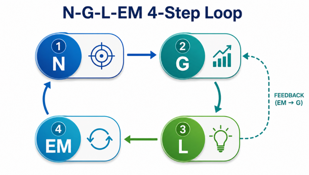
I now strongly recommend that the R & D team introduce this design framework called N-G-L-EM. This methodology directly eliminates the old linear design method and replaces it with a closed-loop co-simulation model. Following this process, you can basically ensure that the physical hardware and software forecast data you deliver are closely matched.
Step 1: Device Selection and DC Bias
Choosing the right active device directly determines the absolute lower limit of the noise figure of your system. For ultra-low noise requirements in the frequency band below 6 GHz, GaAs pHEMT devices are currently basically the world. However, if your application environment is harsh and you need to resist great input power, GaN devices are often a safer choice.
Here is my personal compulsion: when biasing transistors, the eyes must be on “low noise” rather than “maximum gain”. The exact drain current and drain voltage at the lowest noise level will be clearly stated in the manufacturer’s data sheet. As long as you deviate from this particular static operating point, the optimal noise parameters will be unrecognizable. I strongly recommend directly on a set of active bias control circuit, no matter how the temperature floats, the drain current stuck at a fixed value.
Step 2: Source Traction and Noise Figure Circle
To minimize noise, it is necessary to present an optimal noise impedance at the gate of the transistor. The specific approach is to draw the noise figure circle on the Smith chart, and then design an input matching network to accurately push the source impedance of 50 ohms to the center of the lowest noise circle.
Of course, when you match in order to pursue extremely low noise, the input return loss will naturally become ugly. After all, in front of the laws of physics, the reflection coefficient of the lowest noise can never be equal to the conjugate complex of the input reflection coefficient.
Step 3: Inductive Source Negative Feedback
The introduction of inductive source negative feedback is to force the best noise point and conjugate matching point closer to solve the long-standing problem of noise and gain matching fighting each other. Add even a little highly specific inductance between the transistor source pin and the PCB ground to pull the best gain point to the best noise point on the Smith chart.
In practice, hardware engineers implement this inductance by tightly controlling the length of the microstrip line leading to the ground. Remember, don’t be silly to weld a discrete inductor, the tolerance error of that thing will be so large that you doubt your life. We have to solve the problem by physically adjusting the position of the.
Step 4: Electromagnetic co-simulation and parasitic parameter extraction
The step of electromagnetic co-simulation is to turn the theoretical components on paper into real copper traces and see how they interact in the physical world. The entire layout is imported into the electromagnetic solver to extract the S parameters of the passive PCB traces.
Plug this S-parameter block back into your schematic, connect your active transistor model, and run through the system simulation. You will immediately notice that the resonant frequency has dropped. At this time, you need to constantly fine-tune the length of the physical traces in the electromagnetic map, iterating over and over again until the results of the co-simulation exactly match your target indicators.
3 Expert Tips To Avoid Prototype Disasters
Textbooks will only teach you basic theory, but as soon as you get to the test bench, those physical layout traps that can ruin the performance of the amplifier will be exposed. The following design techniques are all lessons learned from real money, and doing so can keep your poor design margin.
Tip 1: Suppress out-of-band instability with a resistive-capacitive network
The gain of high-frequency transistors in the low frequency band is usually surprisingly large. When you check the stability factor, make sure that the K value is strictly greater than 1 and the Delta is strictly less than 1 from DC to the maximum oscillation frequency of the transistor. Don’t just stare at the small band where you work.
My approach is to string a parallel resistance-capacitance network in the output matching network. At your RF operating frequency, the capacitor is equivalent to a short circuit, bypassing the resistor directly, thus keeping low noise and high gain. In the low frequency band, the capacitor is disconnected, the signal is forced to pass through the resistor, the excess gain is consumed, and the circuit is completely stabilized.
Tip 2: Look at the self-resonant frequency to pick the isolation capacitor.
Don’t think a 100 picofarad capacitor can be honestly used as a capacitor at 5 GHz. As long as it is a patch element, it is inevitable to have an internal parasitic inductance, thereby generating a self-resonant frequency. Once your operating frequency approaches or even exceeds this point, your blocking capacitor becomes an inductor, directly eliminating your input noise matching. Before each design, be sure to download the patch capacitance measurement files of specific manufacturers and use them in the simulation of matching networks instead of using those ideal capacitance models.
Tip 3: the RF link and power completely isolated
Once the power supply noise leaks into the drain bias line, it will modulate the RF signal, directly destroying your phase noise and raising the system noise floor. It is necessary to build a solid bias decoupling network, which you can do with a capacitor cascade with decreasing group capacitance. Place the smallest capacitor closest to the RF choke inductor. This kind of play can provide a very low impedance into the ground channel for ultra-wideband power interference.
Case Study: 5.8 GHz WiFi 6E LNA EM Co-Simulation
In order to prove to the team the absolute necessity of the electromagnetic layout process, we previously made a 5.8 GHz amplifier design with standard GaAs pHEMT. We deliberately compared the data differences between pure schematic simulation and post-layout co-simulation.
In the ideal schematic, the system predicts a ridiculously false data: an input return loss of negative 22 decibels and a noise figure of 0.85 decibels. As a result, after we extracted the parasitic parameters of copper skin, the center frequency dropped directly by 400 MHz.
Performance Comparison: Schematic vs. EM Extraction vs. Optimized Layout
| Metric | Ideal Schematic | First EM Extraction | Final Optimized Layout |
| Center Frequency | 5.8 GHz | 5.4 GHz | 5.8 GHz |
| Noise Figure | 0.85 dB | 1.45 dB | 0.92 dB |
| S11 | -22 dB | -8 dB | -18 dB |
| Gain | 16 dB | 14.2 dB | 15.5 dB |
Faced with this extracted data, we can only cut the input matching microstrip line by 12 mils, and at the same time cut the number of source ground vias from four to two to control the negative feedback inductance. With the final optimized layout, the hardware performance returned to the target specification honestly.
FAQ
What is the difference between gain matching and noise matching in LNA?
The core of noise matching is to feed the optimal noise impedance to the transistor input terminal to guarantee the lowest noise figure, but the cost is often extremely poor input reflection loss. Gain matching, on the other hand, requires conjugate matching of the input impedance to 50 ohms, pursuing maximum power transmission. In actual engineering, everyone basically relies on source-pole negative feedback to find a balance between these two mutually reinforcing states.
How does source-pole negative feedback improve LNA linearity?
Adding inductance to the source actually introduces negative series feedback. Although this feedback slightly eats up the total gain of the amplifier, it can pull the gain response extremely flat while significantly improving the input third-order intersection cutoff. In this way, even if a relatively large blocking signal is encountered, the transistor is not prone to compression paralysis.
Can I use VNA to directly measure the noise figure of LNA?
Ordinary vector network analyzers measure S parameters, but they cannot measure thermal noise power at all. You’ll have to get a dedicated noise figure analyzer with a calibrated noise source, or one of those incredibly high-end new network analyzers with specialized noise figure measurement options and low-noise receivers.
What should I do if I find that the K factor of LNA is less than 1?
If the stable K-factor falls below 1 in any frequency band, your amplifier is in conditionally stable state. As long as the source impedance and load impedance catch up to a certain combination, the circuit will vibrate into a transmitter every minute. The solution is to force the addition of resistive load or resistive feedback to force the K factor of the entire frequency band to above 1.
Why do veteran designers prefer coplanar waveguides over microstrip lines?
At high frequencies, grounded coplanar waveguides provide excellent isolation and lower radiation losses. The ground planes on both sides of it can lock the electric field lines tightly, which not only reduces parasitic coupling to other components, but also allows designers to more accurately control the tiny negative feedback inductance at the transistor pad.