 Neditek
Low Noise FET Amplifier: 5 Circuit Diagram Secrets
The core secret of Low Noise FET Amplifier is to guide weak signals through a carefully designed input noise matching network , and use the source Degeneration Inductor to realize the conversion of real impedance without increasing thermal noise, so as to squeeze the noise figure below 1dB while providing high gain.
Many people got the classic low noise amplifier circuit diagram to carry out the construction according to the drawings, but the measured bottom noise was 10dB higher than the original. The problem is not the batch difference of the FET chip itself, but that you ignore the compromise mechanism of RF bias, parasitic parameter control and impedance matching hidden in the schematic. Next, I will disassemble these 5 circuit diagram design secrets that only senior RF engineers can understand.
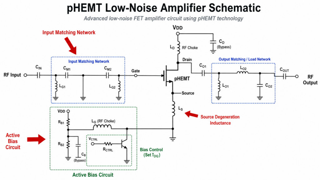
“N-G-S Inverted Triangle Model” For FET LNA Design”
The most common mistake junior circuit design engineers make is to tune a low-noise amplifier as an ordinary amplifier. The correct development logic must follow the N-G-S inverted triangle model.
- N (Noise) noise first: the only primary goal of the matching network is to approximate Γ o p t Γ option. Never pursue an absolute 50 ohm conjugate match at the input (VSWR = 1).
- G (Gain) gain compromise: After meeting the optimal noise figure, the gain will inevitably fall back. The transconductance of the FET ( g m g m ) determines the upper limit of the gain, which you need to compensate by inter-stage matching.
- S (Stability) Absolutely Stable: Broadband FETs are highly susceptible to self-oscillation in the low band. A resistive load must be introduced at the periphery of the drain or gate to lower the Rollett stability factor of the low frequency band to greater than 1.
Analysis Of 5 Core Circuit Diagram Secrets
In any 1 professional low noise fet amplifier drawing, the arrangement of components hides mystery.
The source-to-ground inductance on the schematic is never intended to filter out low-frequency noise, but rather to generate a noise-free real input impedance.
When a high-frequency signal flows through the FET, the source inductance passes through the gate-source capacitance Feedback a frequency-dependent real impedance. This method does not require any real resistance in series at the input. But in reverse engineering, testers often ignore the via parasitic inductance on the PCB. Excessive source inductance will severely reduce the high-frequency gain and even cause parasitic oscillation.
Do not use simple resistor voltage division to power the gate.
The high-end low noise amplifier circuit diagram uses an additional PNP transistor to form a constant current source to directly monitor and lock the drain current of the FET. The optimal noise figure of a FET is strictly dependent on the specific drain current . As the temperature increases, the threshold voltage of the FET will drift, and the active bias can dynamically adjust the gate voltage to ensure that the noise floor remains constant between -40°C and 85°C.
| Parameter | Normal JFET (@ 1GHz) | Modern E-pHEMT (@ 1GHz) |
| Noise Figure (NF) | High (~2.0 dB – 4.0 dB) Inherent device noise dominates. Not sensitive enough to be affected by minor PCB dielectric losses. | Ultra-Low (~0.3 dB – 0.8 dB) Highly sensitive. Any physical loss at the input adds 1:1 to the NF. Standard FR4 eats 0.3–0.5dB of noise margin, requiring careful layout. |
| Gain | Low (< 10 dB) Performance degrades significantly as 1GHz approaches the cutoff frequency of standard JFETs. | High (15 dB – 22+ dB) Delivers excellent high-frequency gain, provided that source parasitics are strictly managed. |
| Input Impedance Matching Difficulty | Moderate / High Loss Often requires real resistance in series at the input for matching, which introduces unwanted thermal noise. | High (Inductive Degeneration) Relies on source-to-ground inductance interacting with gate-source capacitance to generate a noise-free real input impedance. Extremely sensitive to ignored via parasitic inductance, which can severely reduce high-frequency gain and trigger parasitic oscillation. |
| Applicable Scenarios & Biasing Requirements | General-Purpose / Low-Cost Circuits Mostly used for sub-500MHz applications. Gate biasing can be easily achieved using simple resistor voltage division. Standard PCBs are acceptable. | High-End Low Noise Amplifiers (LNAs) Requires active bias (e.g., a PNP transistor constant current source) to directly lock the drain current and dynamically adjust gate voltage against temperature-induced threshold drifts (-40°C to 85°C). Requires Rogers high-frequency plates or hollowing out the reference ground plane directly below the input trace to minimize insertion loss. |
Any physical loss at the input adds 1:1 to the noise figure.
The inductance and capacitance parameters on the drawing are ideal, but in actual wiring, PCB made of FR4 will eat about 0.3dB to 0.5dB of noise margin in the frequency band above 2GHz. Top engineers will use Rogers high-frequency plates at the input end, or hollowing out the reference ground plane directly below the input trace during wiring to reduce parasitic capacitance between the trace and the ground, thus minimizing input insertion loss.
If you need extremely high operating bandwidth, the single FET amplifier will be Miller capacitor limit death.
In broadband RF or high-precision audio sensor drawings, you will see two FETs in series. The lower tube is responsible for providing transconductance without voltage gain, which completely eliminates the amplification effect of Miller capacitance; the upper tube is responsible for providing voltage gain. This topology not only broadens the bandwidth, but also greatly improves the isolation from the output to the input, making it easier for the amplifier to achieve unconditional stability.
The series resistance and capacitance at the output of the drawing are not only for impedance matching, but also for consuming low-frequency gain.
The gain of the FET increases sharply as the frequency decreases. If not suppressed, the amplifier will oscillate strongly in the tens of MHz band, causing the noise floor of the entire band to rise instantaneously. Inserting a low-frequency bypass resistor into the drain matching network can effectively consume these dangerous low-frequency energy without affecting the output of the target high-frequency signal.
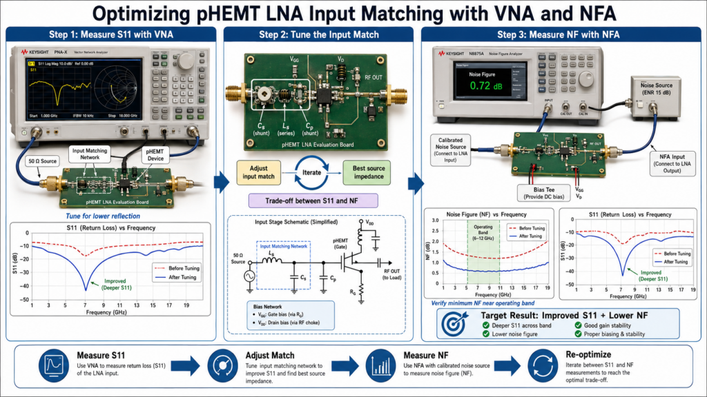
0.8dB NF pHEMT Low Noise Amplifier Measured
Theories must be subordinated to measured data. Our laboratory has designed a low-noise amplifier operating at 1.5GHz based on the ATF-54143 pHEMT, optimized using the above 5 secrets.
Test results show:
- Input Standing Wave Ratio (VSWR): The intentional mismatch is adjusted to 1.8:1 (compromising S11 for best noise).
- Noise figure (NF): 0.78dB measured at room temperature.
- Small signal gain (S21): 16.5dB.
- OIP3 (output third-order intermodulation): 32dBm (thanks to precise active bias locking I d = Sixty m A I d = 60mA ).
If we follow the novice’s thinking and forcibly match S11 to better than-20dB (VSWR < 1.2:1), the measured noise figure will immediately deteriorate to 1.4dB, losing the core value of the low noise amplifier.
FAQs
Q1: Why Is An LNA Input Not Matched Exactly To 50 Ohms?
Matching to perfect 50 ohms is for maximum power transfer, but this is not a condition where the device produces the least noise. The low-noise amplifier must be matched to the “best noise impedance” of the device, which usually causes the input return loss to look less than perfect.
Q2: What Is The Difference Between A Bipolar Transistor LNA And A FET LNA?
FET LNAs have very high input impedance and produce little shot noise, so they can achieve a lower noise figure than bipolar junction transistors in low-frequency high-impedance sources or high-frequency microwave bands.
Q3: How Do I Read An Active Bias Network In A Low Noise Amplifier Circuit Diagram?
Look for a PNP triode next to the main FET in the circuit diagram. The emitter of the transistor is usually connected to the main power supply, and the collector is connected to the FET gate bias circuit. Its role is to sample the drain current of the FET and dynamically adjust the gate voltage to maintain a constant current when the temperature changes.
Q4: Can I Use FR4 PCB Material For A 2GHz Low Noise FET Amplifier?
It can be used, but the price must be accepted. The higher dielectric loss tangent of FR4 will cause an insertion loss of about 0.2-0.5dB at the input. For designs that are extremely pursuing sub-1dB noise figure, it is recommended to use RF special plates such as Rogers 4350B.
Q5: What Happens If The Source Degeneration Inductor Is Too Large?
Although the source degeneration inductance is too large, it can increase the real impedance of the input terminal, but it will excessively reduce the high-frequency gain, and even lead to high-frequency parasitic oscillation due to parasitic effects, which will destroy the overall stability. Usually this inductance is only about 1nH to 3nH, and even the via length on the PCB can be achieved.
Q6: How To Stop My FET LNA From Oscillating?
First check the low-frequency stability of the output. A small resistor of tens of ohms in series on the drain bias line, or the addition of a gate loss circuit containing an RC network, can effectively absorb the excess gain at low frequencies and suppress self-oscilla