 Neditek
Si vs SiC MOSFET: Why Top Engineers Are Switching
Today’s top hardware teams are collectively abandoning traditional silicon (Si) MOSFETs and switching to silicon carbide (SiC). Although SiC is really expensive based on the chip quotation alone, it can reduce the system volume by 40% and greatly cut down the heat dissipation cost.
However, if you directly weld the SiC tube 1 a high-speed switch to the old PCB previously painted on the silicon tube, there is usually only one result: serious electromagnetic interference (EMI) leads to direct explosion of the machine and the drive together. To get on a wide bandgap semiconductor, the entire power circuit must be pushed back and forth. Today, let’s open the parameter table and talk about the accounting logic behind it, the dark pit of PCB wiring, and the real hardware selection doorway.
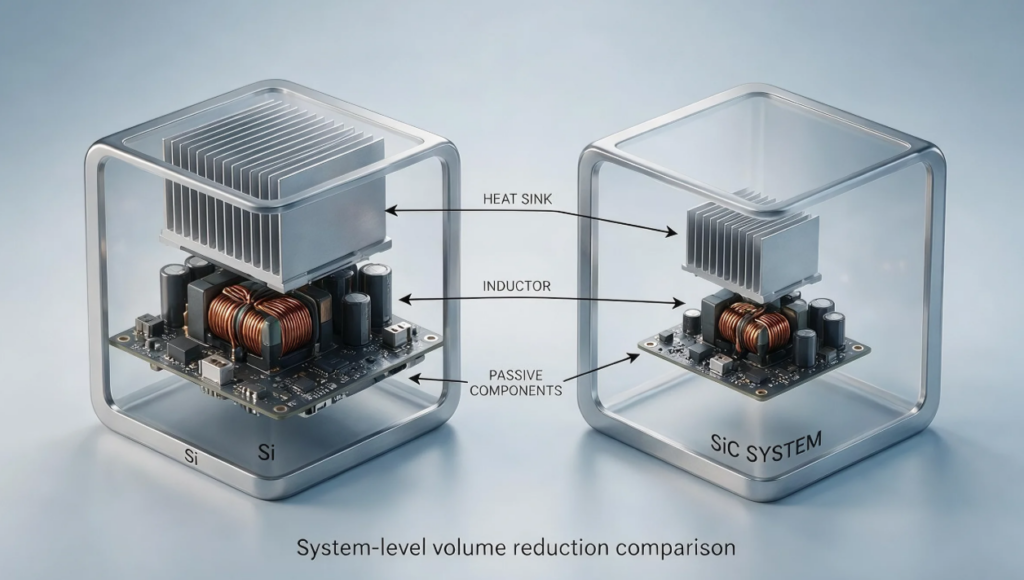
Outside the parameter table: calculate the general ledger of a system-level BOM.
Procurement generally only focuses on the unit price of a single device, but the head of research and development looks at the total BOM (bill of materials) cost. The 1200V SiC MOSFET is indeed more expensive than the silicon super junction MOSFET or IGBT of the same specification. But don’t forget, the switching frequency of SiC can easily run above 100kHz (traditional silicon tubes are generally pressed at about 20kHz), which means that the volume of inductors, DC bus capacitors and radiators can be greatly reduced.
Internally, a benchmark test was conducted on the 1 11kW on-board charger (OBC) in 2025: after replacing the third generation SiC architecture, the switching loss was directly killed by 73%. Because of the soaring efficiency, the R & D team decisively removed the expensive liquid-cooled plate and replaced it with a pure passive aluminum heat sink. According to the calculation, although the SiC chip cost an extra US $40, the saved liquid cooling system and reduced inductance helped cut the cost of the peripheral hardware by US $115. Therefore, to evaluate the economic accounts of silicon and silicon carbide, we should look at the board area of the whole converter, rather than looking at the purchase details of a single line.
EMI Trap: How to survive the “wiring nightmare” brought by dv/dt”
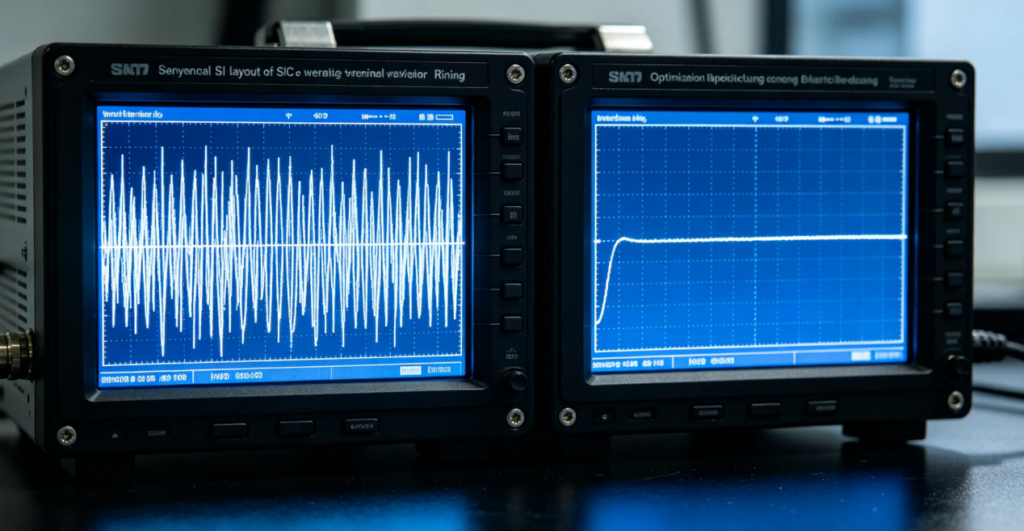
The pit that many novices most often step on is to replace SiC directly as the “perfect flat replacement” of silicon tubes, which is usually the culprit of the early prototype fryer. The switching speed of SiC is extremely fast, and the voltage change rate (dv/dt) often breaks 50V/ns. Once this high-frequency transient voltage hits the parasitic inductance in the ordinary PCB trace, it will stimulate the terrible voltage spike and serious high-frequency EMI.
To survive in the SiC era, Layout (wiring) must be greatly changed. You have to cut the area of the drive loop to the extreme, and the parasitic inductance is dead within 5nH. In addition, the Kelvin (Kelvin) source trace is a rigid design, and a high-current power loop must be completely separated from a fragile gate drive signal. If you don’t care about loop isolation, misleading and straight-through short circuits will follow one after another, and the half bridge will explode directly in situ during the on-load test.
T.C.E. Decision Pyramid: Should We Be on SiC or Not?
In order to filter out the overblown marketing in the market, the old drivers usually use the “T.C.E.(heat dissipation, system cost, efficiency) pyramid” to evaluate whether the project needs SiC or not.
Bottom layer: heat density death. First look at how tightly your device’s appearance and size are stuck. The thermal conductivity of SiC is about 120W/mK, which is almost three times that of silicon. If your industrial motor drive or aviation actuator can’t plug the heavy extruded aluminum radiator at all, then there is no choice. SiC is the only way to prevent thermal runaway.
Mid-level: stringent energy efficiency regulations. For example, to meet the 80 PLUS titanium gold certification, or to cope with the extremely demanding Euro 7 electric vehicle energy efficiency targets. The body diode of SiC has almost no reverse recovery charge (Qrr). In the continuous conduction mode (CCM) topology of totem pole PFC, removing Qrr can save a lot of turn-on losses and enable your product to fly firmly within the regulatory red line.
Top level: System cost balance point. This upgrade is only cost-effective when the money saved from copper (magnetic components) and aluminum (heat sinks) can smooth the difference in SiC chips. Like the kind of ordinary consumer-grade fast charge below 65W, just be honest and practical silicon tube. It is totally overqualified to knock the wide forbidden band there, and it cannot be calculated.
T.C.E. Selection Evaluation Table
| Application Scenario | Si Performance Score (T.C.E.) | SiC Performance Score (T.C.E.) | Final Recommendation |
| Compact Industrial Drive / Aviation Actuator(Severe space constraints) | 3 / 10(Requires bulky extruded aluminum heatsinks; High thermal runaway risk) | 9 / 10(120W/mK thermal conductivity; Solves heat density bottleneck) | Upgrade to SiC |
| 5G Base Station / Server Power(CCM Totem-Pole PFC, 80 PLUS Titanium) | 4 / 10(High Qrr restricts efficiency; Fails to meet stringent regulations) | 9.5 / 10(Near-zero Qrr; Reduces turn-on losses; Meets regulatory red lines) | Upgrade to SiC |
| 800V EV Inverter(Euro 7 targets, System weight reduction) | 5 / 10(High switching losses; Requires massive cooling systems) | 9 / 10(High efficiency; Savings on copper/aluminum offset SiC chip cost) | Upgrade to SiC |
| <65W Consumer Fast Charger(Strict cost control, Standard efficiency) | 9 / 10(Honest and practical; Best system cost balance) | 4 / 10(Total overkill; Cannot justify the chip price premium) | Stick to Si |
How do the underlying physical properties affect the landing of the project?
Band gap and breakdown voltage
The forbidden band width of silicon carbide is 3.26 eV, while silicon is only 1.12 eV. This determines at the atomic level that SiC can withstand the same voltage with a much thinner drift layer. For engineers, the most direct benefit is that it has a surprisingly low on-resistance (Rds(on)) in the critical voltage range of 1200V. This is also why the 800V high-voltage platforms of various car companies are now scrambling for SiC, because it perfectly avoids the fatal weakness of exponential increase in conduction loss of high-voltage silicon devices.
Thermal stability under heavy load
The traditional silicon tube 1 over 150 ℃, the internal intrinsic carrier concentration will surge, easily lead to thermal runaway. However, even if the junction temperature of SiC is above 200 ℃, Rds(on) is still as stable as an old dog. This extremely strong thermal stability makes it easy to perform under the harsh conditions of photovoltaic string inverters and traction motors that are always full or even overloaded for a long time.
Parasitic Capacitance and Driver Design
Because the specific on-resistance is small, the wafer area of SiC can be made smaller under the same current, which naturally reduces those annoying parasitic capacitances (Ciss, Coss, Crss). Coss is small, the charging and discharging of the switch node is fast, which directly reduces the switch overlap loss. However, this also forces us to use more accurate asymmetric driving voltage (for example, 15V for opening and -4V for closing) to resist high dv/dt transients and prevent accidental conduction caused by Miller effect.
Frequently Asked Questions (FAQ)
What is the biggest advantage of SiC over ordinary silicon MOSFETs?
Simply put: At extremely high temperatures, switching losses and conduction losses can still be greatly reduced. This directly determines that your power system can be made smaller, lighter, and more power-dense.
Can I directly unplug the silicon tube on the board and insert a SiC?
Absolutely not. SiC switching speed is too wild (dv/dt is extremely high), it must be equipped with a special gate driver with negative pressure shutdown, and it must be matched with extremely exquisite PCB wiring to suppress parasitic inductance, otherwise it will inevitably cause serious ringing and even EMI explosion.
What is the best value for a system with SiC?
650V to 1700V this range, SiC is the absolute king. If it is below 400V, the cost performance of ordinary silicon tubes is still invincible. However, in the extreme heavy industry scenario of 1700V, it is still the world of high-end silicon IGBT modules or special SiC modules.
Does a SiC MOSFET have a body diode?
There is some. And its body diode reverse recovery charge (Qrr) is extremely low. This feature minimizes unnecessary waste of energy when switching in half-bridge or full-bridge circuits.
Why are silicon carbide chips so expensive?
Because silicon wafers can be quickly “pulled” out, and silicon carbide ingots must be in a special furnace above 2000 ℃, with sublimation method a little bit “long” out. This stuff is extremely expensive and slow to grow, resulting in a naturally high production cost for bare dies.