 Neditek
GaN vs SiC MOSFET: Which Suits Your Power Designs?
Silicon carbide (SiC) MOSFETs dominate in high-power, high-temperature applications above 800V (such as traction inverters for electric vehicles), while gallium nitride (GaN) shines in designs below 650V that require ultra-high frequencies and are limited in size (such as communication power supplies and lidars). But the real headache for hardware engineers is actually the “overlapping blind area” of 650V to 900V “. In this range, once you choose the wrong wide band gap (WBG) device, your thermal budget will directly explode, EMI filtering costs will increase exponentially, and the reliability of the entire system will suffer. In this article, let’s not talk nonsense, skip the basic chemical materials science popularization directly, and cut neatly from the hard core engineering indicators to help you select the most suitable device for the specific topology.
V-F-T Boundary Model: Underlying Logic for Device Selection
Many R & D teams often spend weeks on the question of “choosing GaN or SiC”. The fundamental reason is that they always look at the parameters in isolation. In fact, using the V-F-T (voltage, frequency, thermal) boundary model, you can accurately match your actual application requirements with the physical limits of the device.
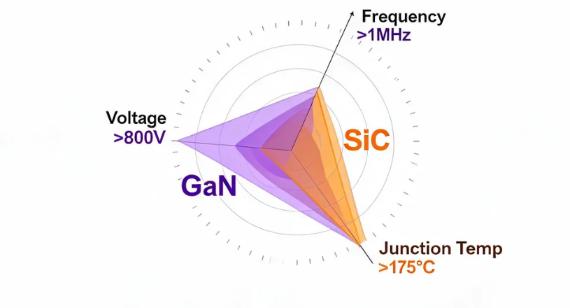
Step 1: Find out the voltage ceiling (V). SiC is very strong in longitudinal voltage spread. If your bus voltage exceeds 800V and requires high avalanche tolerance, just choose SiC with your eyes closed. On the other hand, GaN devices, because they are mainly lateral HEMT structures, naturally lack avalanche tolerance and can only rely on transient overvoltage rating, which requires extremely strict clamping of bus voltage during design.
Step 2: Determine the frequency target (F). GaN has a killer-reverse recovery charge (Qrr) is zero. If your topology needs to increase the switching frequency above 500kHz to reduce the volume of magnetic components, GaN can directly eliminate the turn-on loss. For SiC, this high-frequency loss would have paralyzed the entire design.
Step 3: Calculate the heat dissipation capacity (T). The thermal conductivity of SiC is three times that of silicon, and the GaN substrate is completely crushed. If the product size limits the space for active heat dissipation, or the junction temperature (Tj) is always up to 175°C, the SiC package can still be as stable as an old dog. In this case, GaN often requires an extremely complex bottom heat dissipation design.
GaN vs. SiC MOSFET: What are the differences in hard core engineering?
The data sheets of various manufacturers are boasting about how low their on-resistance (RDS(on)) is, but to be honest, in practical applications, dynamic performance is the hard indicator that determines true efficiency.
Switching Dynamic Characteristics: Ultra-High Frequency VS High Avalanche Tolerance
In the field of ultra-high frequency, GaN is definitely the king. GaN HEMT as a two-dimensional electron gas (2DEG) device, its gate charge (Qg) and output capacitance (Coss) is surprisingly small. You can push a GaN-based active clamp flyback (ACF) converter to 1MHz with minimal switching losses. In contrast, SiC MOSFETs are much faster than traditional IGBTs, but they have higher parasitic capacitance. If you pull the operating frequency of SiC above 200kHz, you will have to knock down the capacitor switching loss (Eoss).
Thermal Management: Turn-On Capability At Junction Temperature Spikes
SiC is simply the most tolerant device of “thermal abuse. The excellent thermal conductivity of silicon carbide allows engineers to run large continuous currents on a very small wafer area. Even if the junction temperature (Tj) reaches 150 ° C., the RDS(on) of SiC is significantly less deteriorated than that of GaN. However, the lateral structure of GaN will cause all heat to accumulate on the wafer surface. In high-power applications, GaN must rely on radical copper clip package or double-sided heat dissipation scheme, otherwise local thermal runaway will teach people every minute.
Gate Drive Design: Parasitic Inductance Sensitivity Vs. Negative Bias Requirements
Drive design is the most tit-for-tat place in the debate between the two. GaN’s requirements for PCB wiring can be called “surgical level” precision. Ordinary GaN gate threshold voltage is extremely low (about 1.5V), even with a little parasitic source inductance (Ls), coupled with extremely fast dV/dt (up to 100V/ns), will cause serious gate oscillation and misleading.
As for SiC, its gate drive is a completely different set of voltage management logic. In order to ensure clean turn-off and prevent false triggering caused by Miller capacitor, SiC MOSFET usually needs a negative turn-off voltage (such as -4V) and a high turn-on voltage (15V to 18V) to fully enhance the channel, thus minimizing the turn-on loss.
650V class chaos bucket: SiC and GaN hand in hand
The most maddening design choices often occur at the 650V node. As the costs of the two converge, system architects can no longer make decisions simply by looking at the price tag.
Data Center Power (CRPS): Totem PFC is now a big fan of GaN. In the past, in the continuous conduction mode (CCM) totem pole PFC, the hard switching loss of traditional silicon devices is simply horrible because of the reverse recovery problem of the body diode. With the advantage of zero Qrr, GaN can easily exceed 99% of the peak efficiency of server power supply above 3kW, directly reducing the volume to the level of meeting the 80 Plus titanium gold medal standard.
Electric vehicle on-board charger (OBC): two-way OBC is entirely SiC’s site. This type of system has to handle 11kW to 22kW of power and works in a harsh car-gauge environment with extremely high coolant temperatures. SiC’s strong short-circuit withstand time (SCWT) and excellent heat capacity provide the reliability necessary to meet automotive functional safety (ISO 26262).
Avoidance Guide: What the Data Book Doesnot Tell You
When the beautiful data in the laboratory meets the real field conditions, the device selection is often easy to roll over. The following several engineering circles often step on the pit, must walk around.
Pits in GaN: Dead time conduction traps. GaN has no physical body diode. In the dead time of the half-bridge circuit, it is turned on in the reverse direction by the channel, which will produce a huge voltage drop (depending on the gate off voltage, VSD can even exceed 2V to 3V). If your underlying software leaves a wide dead time to be conservative, the reverse conduction loss will instantly eat up all the efficiency dividends you save by fast switching. Cracking scheme: Be sure to add adaptive dead time control.
Pits of SiC: threshold voltage (Vth) shift. The gate oxide layer of SiC is easily affected by the charge trapping effect. Under thousands of hours of high-frequency AC stress, its Vth will inevitably drop. This leads to a SiC MOSFET that can be safely turned off at 0V, and parasitic conduction may suddenly appear. Solution: When designing SiC gate drive, always remember to add active miller clamp and give a reliable negative bias (-3V to -5V).
Measured data speak: 11kW phase shift full bridge topology
We ran a benchmark test in which we replaced the original SiC module with a parallel GaN architecture in an 11kW phase-shifted full-bridge (PSFB)DC-DC converter.
| Metric | 1200V SiC MOSFET | 650V GaN HEMT (Paralleled) |
| Max Frequency Achieved | 120 kHz | 350 kHz |
| Magnetics Volume | Baseline (100%) | Reduced by 42% |
| Cooling Requirement | Standard Liquid Plate | Advanced Double-Sided |
| Gate Drive Complexity | Medium (Isolated, -4V/+15V) | High (Kelvin Source, isolated, strict layout) |
| Peak Efficiency | 97.8% | 98.4% |
The final result: thanks to the 350kHz high-frequency switching capability, the GaN scheme has cut the volume of magnetic components by 42%. But don’t be too happy-in order to adjust PCB wiring and eliminate gate oscillation in GaN parallel architecture, our hardware team spent more than three times as long as SiC integration. The conclusion is very straightforward: if you want to knock down the power density, choose GaN; If you want the product to go on the market quickly, plus high-power thermal stability, please choose SiC.
Frequently Asked Questions (FAQ)
Q: Are there body diodes for GaN and SiC?
A: SiC MOSFET has an intrinsic body diode, and its reverse recovery characteristic is very resistant, although the speed is slightly slower. However, GaN HEMT has no physical body diode at all. It conducts reverse current directly through the 2DEG channel, and the reverse recovery charge (Qrr) is zero. This makes it extremely efficient in a half-bridge hard-switching topology.
Q: Why does the current 800V electric vehicle inverter not use GaN?
A: At present, the commercial lateral GaN structure on the market is difficult to keep the wafer size and cost advantages while pulling up the rated voltage to 1200V. In contrast, SiC has great advantages in longitudinal withstand voltage expansion, and the avalanche energy is extremely high, which is absolutely necessary when the heavy-duty vehicle traction inverter absorbs load dump (load dump).
Q: Can I use a standard SiC gate driver to push a GaN MOSFET?
Answer: Absolutely not. The SiC driver usually outputs a turn-on voltage of 15V to 18V and a negative turn-off voltage. If you dare to add 15V to the gate of standard enhanced GaN, the device will burn out instantly, because the absolute maximum voltage of its gate is generally clamped to about 6V to 7V.
Q: Is GaN or SiC cost effective for a 3kW communication power supply?
A: At the 3kW level, GaN’s system-level price/performance ratio is better. Although the cost of the two dies is very tight, GaN can make the totem pole PFC easily run at frequencies above 100kHz, greatly reducing the size and cost of inductors and EMI filters.
Q: How does the short-circuit capability of SiC and GaN compare?
A: SiC MOSFETs usually have a definite short-circuit withstand time (SCWT), usually about 2 to 3 microseconds, which gives the driver IC enough time to detect and cut off the circuit. However, once the GaN device is short-circuited, it will enter the saturation region very quickly. SCWT is very short and must be equipped with a set of exclusive overcurrent protection circuit with ultra-fast response.