 Neditek
What Is Mosfet In Electronics
In the field of modern power electronics, especially in the demanding automotive, aerospace and industrial automation industries, MOSFET is not a new term, it is the core cornerstone of efficiency and reliability. Too many people think of it as just a three-terminal semiconductor switch, but in fact, it is a precision-designed voltage-controlled device. The core task is to handle high-frequency switching and power conversion with very low loss.
MOSFETs have 3 key pins: Gate, Drain, and Source. Its working logic is to apply a voltage to the gate to generate an electric field, which in turn controls the current between the drain and the source. In high-performance systems such as electric vehicle motor drives, smart grid inverters, and aerospace power distribution, we often abandon the traditional BJT in favor of MOSFETs, mainly because of its extremely high input impedance, fast switching speed, and better thermal stability. If you are looking for NEDITEK that level of reliability, then your focus must be on how to optimize RDS and Gate Charge, only in order to drain the power density of the system under extreme conditions and ensure that the equipment can run for a long time.
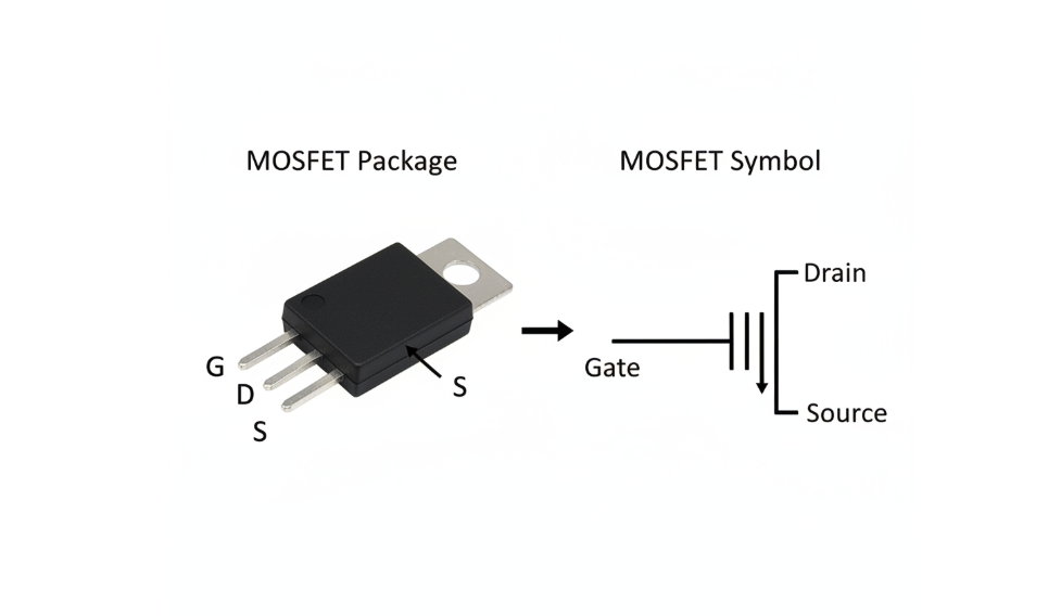
Control Architecture: Gate, Drain, and Source
In terms of physical structure, the three-terminal architecture of a MOSFET determines the upper limit of its performance. If you want to understand MOSFETs in electronic circuits from a professional perspective, you have to dig deep into the internal physical logic of these connection points:
- Gate: This is the “command post” for the entire device. Because the gate is insulated from the main semiconductor channel by a very thin layer of silicon dioxide, it produces an extremely high input impedance. This means that as long as the voltage is in place, it can maintain the “on” state with almost no continuous current, which is completely different from the “current eating” base of BJT.
- Source and Drain: This is the main battlefield of power flow. In the most common N-channel devices, as long as the gate voltage is satisfactory, electrons will travel from the source to the drain.
When I’m dealing with cases of aerospace or exploration systems, the integrity of this oxide layer is an absolute red line. The reason why the NEDITEK level standard emphasizes the strength and toughness of the insulating layer is to prevent gate leakage under extremely strong electromagnetic interference.
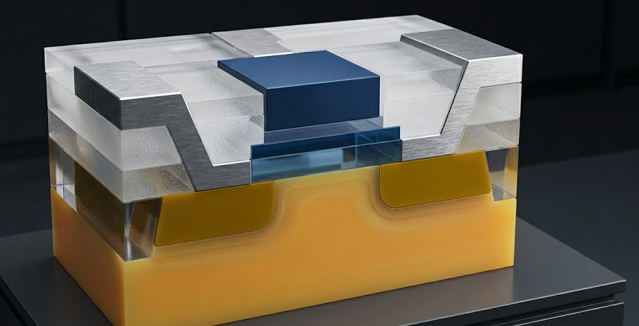
Efficiency and High Frequency Characteristics Brought by Voltage Control
Why MOSFET can become the standard of automobile and new energy industry? The key is that it is voltage control. Unlike bipolar transistors, which rely on minority carrier injection, it is the majority carrier device.
- Extreme switching: Because there are no stored carriers that need to be removed when switching off, the switching frequency of MOSFETs can soar to the hundreds of kHz or even MHz level.
- Extremely low switching losses: High-frequency operation means that we can use smaller passive components such as inductors and capacitors, which is essential for mobile terminals or microdisplays to pursue extreme sizes.
Optimize RDS and Qg for Power Density
There are two indicators that cannot be bypassed: RDS and gate charge. They directly determine the physical limits of the power system.
- RDS: This is the resistance between drain and source in the on-state. The formula for heat loss is simple: P_loss = I²×RDS. In the application of rail transit or smart grid with huge current, even if RDS is only reduced by a few milliohms, the heat dissipation pressure can be greatly reduced and the efficiency of the whole machine can be improved.
- Gate charge: This is the amount of charge that must be injected into the gate in order to fully turn on the device. The lower the Qg, the faster the switch, and the lower the driving power. This is a life-saving straw for battery-sensitive designs such as home appliances or handheld industrial tools.
Thermal Stability and Long-Term Durability in Extreme Environments
The “excellent thermal stability” mentioned in our definition is actually the core logic of MOSFET’s ruling industrial applications. The resistance of a MOSFET has a positive temperature coefficient—the higher the temperature, the higher the resistance. This automatically eliminates the phenomenon of “grabbing current” physically, making it very easy for multiple tubes to handle the high current of the electric vehicle drive system in parallel.
To achieve the reliability of NEDITEK standards, physical characteristics alone is not enough, but also depends on:
- Advanced packaging: must be able to resist the impact of thermal cycling in the engine compartment of the car or rail transit.
- Robustness: The ability to withstand “avalanche” events without catastrophic failure is a requirement for aerospace power distribution systems.
Why Does It Have to Be a High-Performance System
When you compare a MOSFET to a traditional BJT in a high-specification electronic design, the advantages are clear at the system level:
- High input impedance: Simplifies the drive circuit, reduces the number of parts, and directly improves the reliability of the wireless communication infrastructure.
- Top efficiency: In new energy systems, the low conduction and switching losses brought by the optimized MOSFET directly become the user’s ROI.
