 Neditek
High Power PIN Diode Switch: Six Checks Before Selection
In a transmit/receive RF path, a switch has two demanding jobs. It must carry the intended signal with acceptable loss, then isolate the inactive path when the state changes. A diode described as “high power” does not settle either question on its own. The RF circuit, bias supply, switching sequence, board layout and heat path all affect the result.
If you are choosing a high power pin diode switch, begin with the conditions the assembled circuit will actually face. That makes it easier to compare parts without confusing a device rating with a finished switch rating.
Understand What The PIN Diode Does
A PIN diode has an intrinsic region between its P and N regions. With forward bias, it can present a low RF resistance. With reverse bias, its impedance rises. Designers use those states in series, shunt or series-shunt switch circuits. The diode is therefore one part of the switch, alongside the RF path and the circuitry that drives it.
Define the switching function before looking at a part number. An SPST circuit controls one path. An SPDT transmit/receive circuit connects a common antenna port to one of two paths and needs a defined state during the transition. Also record the operating band, whether the signal is continuous or pulsed, the highest expected input power, the likely load mismatch, the loss and isolation targets, and the required RF switching time.
Check Off-State Voltage Against RF Peaks
Average input power is a poor shortcut for selecting reverse voltage. An off-state diode sees an instantaneous RF voltage in addition to its DC bias. Under a mismatched load, the stress at some phases can exceed that seen with a matched 50-ohm termination. The selection process should account for the RF peak, mismatch, bias and control transients, while keeping the device within its stated reverse working-voltage limit.
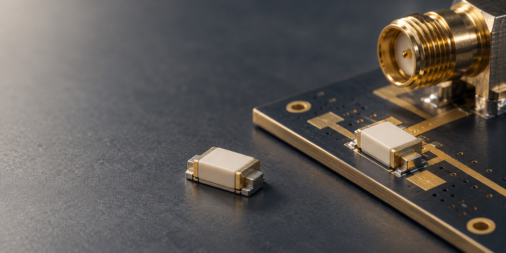
Neditek lists several high-power ceramic leadless surface-mount PIN diodes in BT2101 and BT3601 packages. The NDGD030003, for example, has a listed reverse working voltage of 500 V. That is a value for this part, not a blanket rating for every device in the family or for a switch assembled around it. Neditek also lists separate 2 kV and 3 kV PIN diode ranges intended for high-power HF and VHF switching; their suitability still depends on the chosen part and circuit conditions.
Compare On-State Loss And Off-State Isolation Together
For a series path, RF series resistance at the applied forward current matters to insertion loss. In the off state, capacitance contributes to leakage and limits isolation. A shunt branch may help isolation, but its grounding and board parasitics must be considered. Combining series and shunt elements can improve isolation at the cost of a more involved bias network and layout.
Read the conditions beside every data-sheet value. For NDGD030003, the listed typical total capacitance is 0.35 pF at 1 MHz with 100 V reverse bias. Its typical series resistance is 0.55 ohm at 100 mA forward current and 100 MHz. Those values are useful for an initial comparison. They are not measured insertion loss or isolation for your operating band, bias point and PCB.
Treat The Driver As Part Of The RF Switch
Forward drive must supply enough current for the intended low-resistance state. When switching off, the driver must establish reverse bias and remove stored charge from the intrinsic region. A logic edge at the control input is not proof that the RF path has already reached its specified isolation or insertion loss.
In a transmit/receive design, define the transition so that both high-power paths do not conduct at once and transmit power is not briefly routed into the receive front end. The RF choke, DC blocking capacitor and decoupling elements in the bias network also need suitable frequency, power and bias ratings. Their parasitics can change the performance of the complete circuit.
Verify The Package And Heat Path
Power handling depends on dissipation and the path that carries heat away from the diode. Neditek’s high-power surface-mount family uses hermetic metal-ceramic leadless packages and double-sided chip bonding intended to reduce thermal resistance. That package construction helps frame the choice, but it does not remove the need to check installation, cooling and duty cycle for the specific design.
A beam-lead PIN diode may be attractive when microwave parasitics are especially important. Its low capacitance alone does not establish suitability for continuous high-power service; allowable dissipation and thermal resistance still need attention.
Prove The Choice On The Intended Board
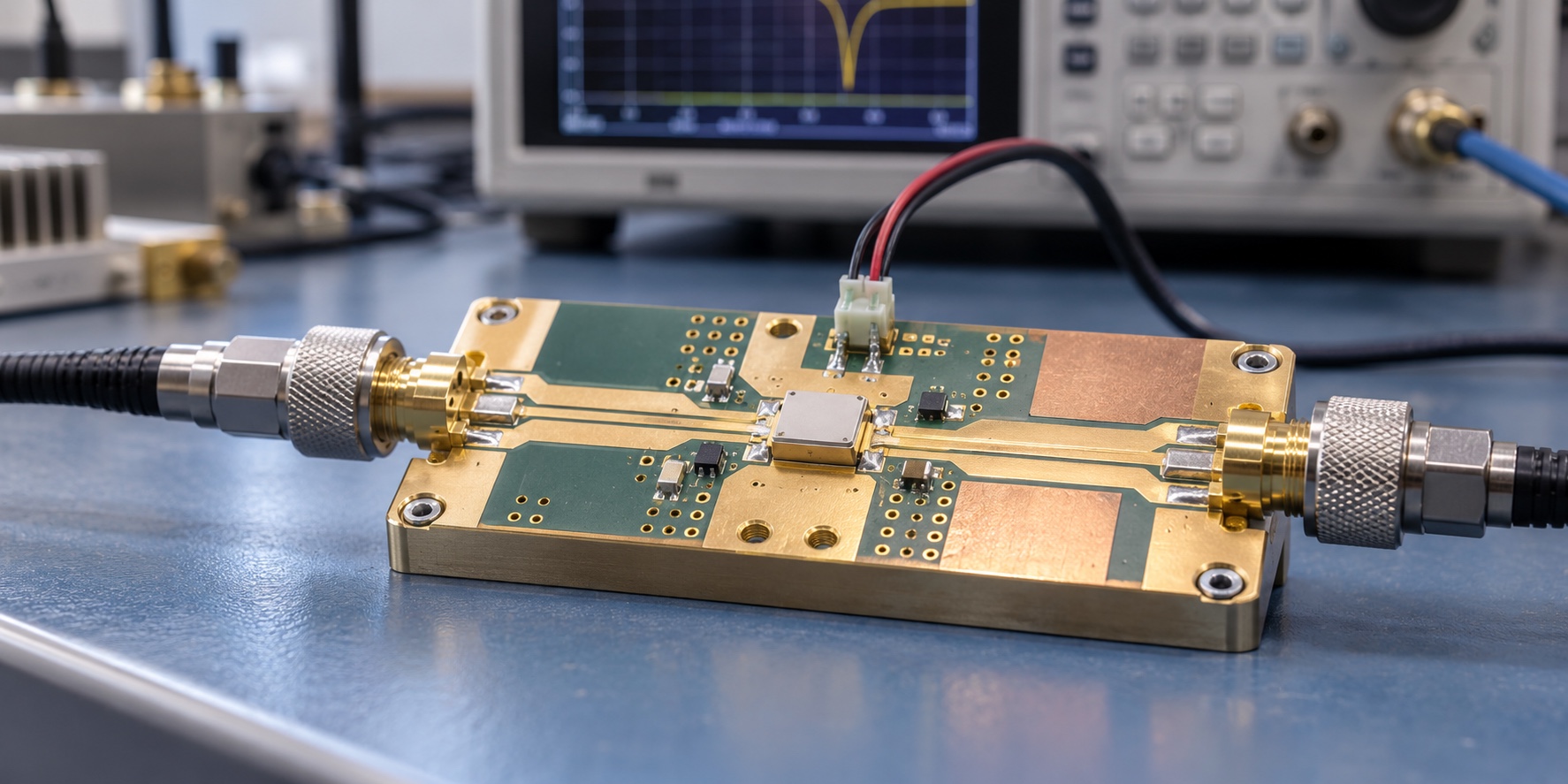
After narrowing the part list, test the assembled switch at the intended frequency and bias. Measure insertion loss, isolation, return loss and RF switching time, then repeat at the relevant high-power, temperature and mismatch conditions. If off-state isolation falls short, investigate reverse bias, charge removal, diode capacitance, driver leakage and coupling across the PCB before blaming the diode itself.
Recording those conditions with the selected part number turns a promising component specification into a useful engineering decision for the complete switch.