 Neditek
How Do Rf Amplifiers Work? From Input To Output
A weak signal reaches an amplifier. A stronger signal leaves it. The part that is easy to miss is where the extra power comes from: the amplifier's DC supply. The RF input controls an active device, while the surrounding circuit helps that device deliver a larger RF signal to the next stage or load.
How do RF amplifiers work in a real system? The useful explanation connects that energy flow with bias, impedance matching and the limits of the active device. Those details explain why more gain does not always produce a better receiver, and why a transmitter cannot keep increasing its output simply by applying more drive.
The Rf Input Controls Energy From The Supply
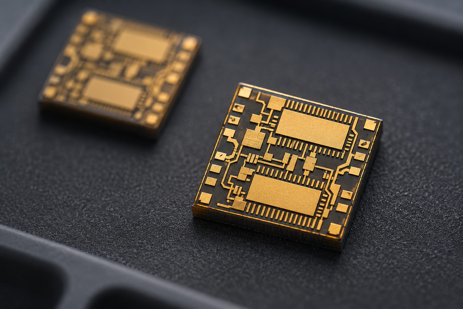
In a transistor amplifier, the input signal changes the current flowing through the active device. In a GaN HEMT, for example, the gate electric field controls the conducting channel between the source and drain. With an appropriate supply and bias, that changing current can deliver RF power to the output network.
The DC supply provides the energy needed for amplification. The input determines how that energy is controlled. This distinction also explains why the amplifier needs a thermal path: power that does not become useful RF output contributes to losses and heating.
The transistor is only part of the circuit. A working RF power amplifier also needs input and output matching, bias feeds, decoupling, stability measures and a suitable thermal structure. A complete solid-state power amplifier may add driver stages, power combining, monitoring, protection and cooling.
Bias Sets The Operating Point
Bias establishes the transistor's operating condition before the RF signal is applied. Changing that condition changes its gain, current consumption, linearity and efficiency. The recommended bias therefore belongs to the particular device and application; it is not a universal setting for every amplifier.
Amplifier classes describe different operating choices. A Class A device conducts throughout the RF cycle, offering a generally linear response with substantial standing power consumption. Class AB conducts for more than half but less than a full cycle, balancing linearity and efficiency. Class C conducts for less than half a cycle and relies on a tuned load to recover the desired fundamental component.
That makes Class C a different choice from a stage intended to reproduce a varying signal envelope linearly. The signal format matters as much as the required output power. A setting that suits one waveform may distort another.
Matching Networks Connect The Device To The System
The impedance needed at a transistor's terminals is not automatically the same as the impedance at an external RF connector. Matching networks connect those two requirements. In a power amplifier, the input network supports the required drive and gain response, while the output network presents an appropriate load to the active device.
There is no single best load for every objective. The load that gives the highest output power may differ from the one that gives the best efficiency or linearity. Matching is therefore part of the amplifier's performance design, rather than an accessory added after the transistor is selected.
These networks are frequency dependent. Transmission lines, pads, package connections and grounding all affect their behavior. A transistor's frequency capability alone cannot establish the bandwidth of a finished amplifier. The complete circuit must meet its gain, power and matching requirements across the intended band.
Gain Describes A Ratio, Not An Unlimited Output
Power gain compares RF output power with RF input power. When the two powers are expressed in dBm, gain in dB is the output value minus the input value.
Consider an illustrative calculation: an input of 0 dBm with 20 dB of gain gives an output of 20 dBm, or 100 mW. This assumes the amplifier remains in its linear operating region at the stated frequency and conditions. It is a calculation example, not a product rating.
At low input levels, an increase in input produces a similar increase in output. As drive rises, the amplifier eventually enters gain compression: the output falls below the value predicted from its small-signal gain. The 1 dB compression point is where the gain has fallen by 1 dB relative to that extrapolated response.
Saturated output power describes a different operating condition. It cannot be substituted for P1dB or treated as a guarantee of clean output with a modulated signal. For signals with high peaks relative to their average level, output backoff leaves room for those peaks, with consequences for average power and efficiency.
A Receiver And A Transmitter Need Different Kinds Of Amplification
An RF power amplifier in a transmitter is designed to deliver the required power to its load while meeting linearity, efficiency and thermal requirements. A low-noise amplifier, or LNA, serves a different purpose near the front of a receiver: it adds gain while introducing as little additional noise as practical.
An LNA does not remove noise already present at its input. Its early gain reduces the relative contribution of noise from later stages. Losses in a cable, filter or switch before the LNA still affect the receiver's noise performance.
More receiver gain also has a limit. A strong unwanted signal can overload the LNA or a later stage. Receiver design needs enough gain for weak signals while preserving headroom for stronger ones. Comparing amplifiers only by their gain misses that tradeoff.
What Changes Between A Chip And A Complete Amplifier?
The same principles apply across different product forms, but the work left to the system designer changes. A bare transistor needs external bias, matching and thermal installation. An MMIC integrates active devices and microwave circuit structures on a chip. A module or complete amplifier incorporates more of the surrounding functions, although its supply, cooling and interface requirements still need checking.
Neditek's RF product range includes amplifier devices and solid-state power amplifier systems. A useful starting point for a discussion is the required product form, frequency band, signal type, input level and desired output. Those requirements help establish whether the project needs a component for a new circuit or a more complete amplifier assembly.
Check The Behavior Under The Conditions That Matter
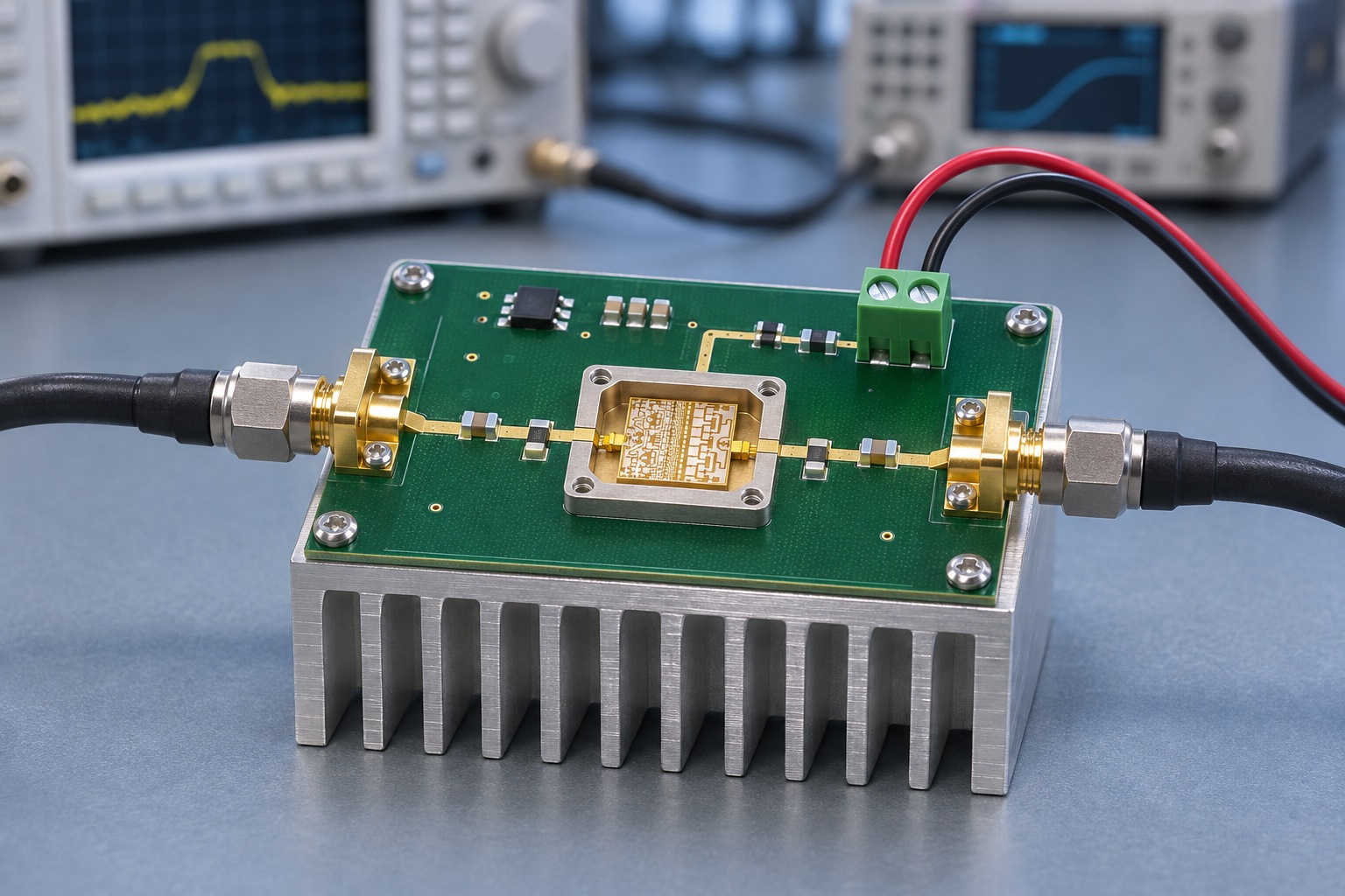
To evaluate an amplifier, specify the operating band and waveform first. Then relate the required output to available drive, gain compression, linearity and cooling. A single power number cannot describe all of those conditions.
Small-signal gain and matching measurements describe one part of the behavior. Output power, compression and efficiency need measurements at the intended drive level. For modulated signals, error vector magnitude and adjacent-channel leakage provide information that P1dB alone cannot supply.
Measurements also need a defined reference plane. Cable, fixture, coupler and attenuator losses can change the apparent gain or output power. Keep those losses accounted for when comparing the amplifier's input and output.
The practical goal is usable amplification: enough signal at the next stage or load, with acceptable distortion, noise and temperature. Once the supply, active device, matching networks and operating limits are considered together, an RF amplifier becomes much easier to understand and specify.