 Neditek
How Does A Low Noise Amplifier Work? 3 Working Secrets
A low noise amplifier boosts a weak radio frequency signal captured by an antenna while keeping self-generated electronic noise to an absolute minimum. This specific function of low noise amplifier circuits ensures that communication receivers can process faint signals from satellites, distant cell towers, or space probes without losing the data in background static. Many junior hardware engineers fail to design these circuits correctly because they rely entirely on ideal simulation software. We will break down exactly how does a low noise amplifier work using real hardware testing principles and bypass the basic textbook definitions.
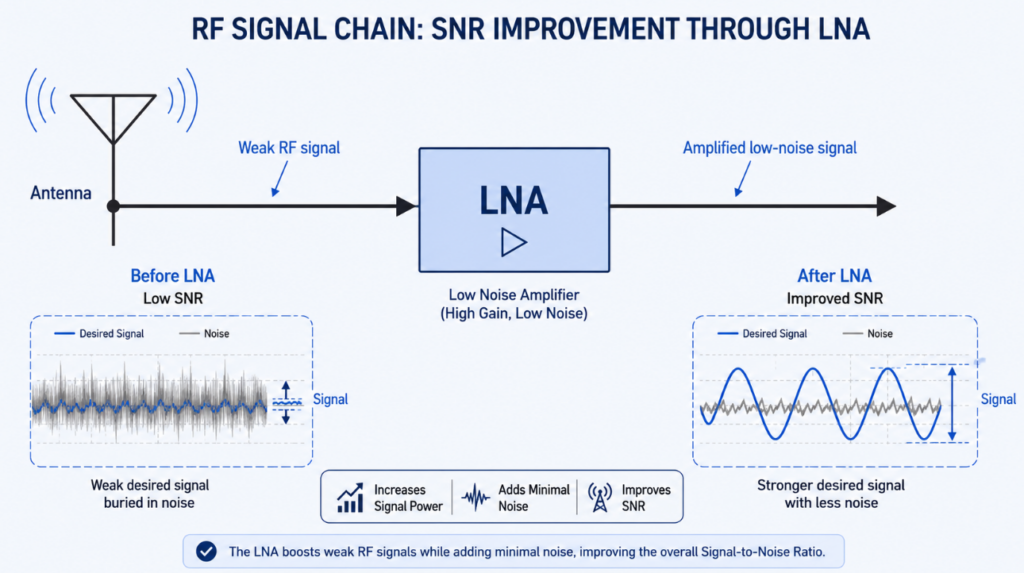
Low Noise Amplifier Theory Explained
Hardware designers view the low noise amplifier theory through a conceptual model called the Signal-to-Noise Ratio Protection Pyramid. This three-layer framework strips away the complexity of radio frequency front-end designs.
Layer One is Impedance Capture. The base of the pyramid focuses entirely on grabbing the maximum amount of voltage from the antenna. If the amplifier input rejects the signal due to a mismatch, the rest of the circuit becomes useless.
Layer Two is Thermal Noise Suppression. Internal components generate random electron movement that creates static. The amplifier uses specialized transistor biasing and precise material selection to keep this internal static from covering up the weak incoming signal.
Layer Three is Linear Drive. The top of the pyramid ensures the amplifier pushes the signal to the next component in the radio chain without distorting the wave shape.
Low Noise Amplifier Working Mechanisms
Understanding low noise amplifier working mechanisms requires looking at the physical layout and the behavior of electrons within the transistors.
Bypassing Thermal Noise At The Input Stage
Every electronic component creates thermal noise. The first active component inside the amplifier dictates the noise level for the entire system. Engineers use field-effect transistors configured in specific layouts to route the signal quickly. They keep the current flow steady. A fluctuating current creates noise. By locking the voltage and current into a specific direct-current operating point, the transistor amplifies the radio wave but adds very little internal electron vibration to that wave.
Achieving Absolute Impedance Matching
The most critical part of low noise amplifier basics is the input matching network. This network acts like a funnel. It matches the resistance of the antenna to the resistance of the amplifier. Engineers use inductors and capacitors at the input stage. They physically arrange these parts on the circuit board to ensure the signal flows into the transistor without bouncing back toward the antenna. A perfect match guarantees the weakest signals enter the amplification stage cleanly.
Managing The Intermodulation Distortion
Strong interfering signals from nearby transmitters often enter the antenna alongside your weak target signal. The amplifier must handle these strong signals without mixing them together. If the amplifier mixes two different radio waves, it creates a third ghost signal that destroys your data. Hardware testers use high biasing currents to keep the transistor in a linear operating region. This linearity ensures the amplifier boosts everything equally without generating ghost signals.
Core Low Noise Amplifier Characteristics You Must Measure
You must evaluate specific low noise amplifier characteristics to determine if your hardware will survive in the real world. Relying on a single specification always leads to hardware failure.
Gain Versus Noise Figure Dependency
Gain tells you how much the signal grows. Noise figure tells you how much static the amplifier adds. High gain typically reduces the impact of noise from later components in the radio chain. However, pushing a transistor to its maximum gain usually increases its own noise figure. Radio frequency engineers select a specific operating point that provides enough gain to drive the system while keeping the internal noise at the absolute floor.
Material Impact: GaN versus Traditional Silicon
Silicon and Gallium Arsenide dominated this field for decades. Modern millimeter-wave hardware and modern base stations now use Gallium Nitride on Silicon Carbide substrates. Gallium Nitride components survive high-power interference that would instantly burn out an older silicon transistor. This material shift allows designers to build amplifiers that handle strong pulse signal while still picking up incredibly faint echoes.
GaN vs GaAs vs CMOS in LNA Design
| Comparison Criteria | GaN (Gallium Nitride) | GaAs (Gallium Arsenide) | CMOS (Silicon) |
| Power Handling | Very High: High breakdown voltage and excellent survivability. Often eliminates the need for input limiters in LNA designs. | Moderate: Lower breakdown voltage. Typically requires external input limiters to protect the LNA from high-power damage. | Low: Very low breakdown voltage. Highly vulnerable to high input power and requires strict protection mechanisms. |
| Noise Figure (NF) | Good / Moderate: Generally higher NF than GaAs, but highly preferred in radar and basestations where survivability is prioritized. | Excellent (Very Low): The traditional industry gold standard for LNAs, offering the lowest noise figure and superior receiver sensitivity. | Moderate: Higher NF than GaAs (especially at mmWave frequencies), but acceptable for mass-market consumer electronics. |
| Integration Capability | Low: Typically used in discrete designs or specific MMICs. Difficult to integrate with dense digital logic on the same die. | Moderate: Good for standalone RF front-end integration (RFICs), but cannot integrate complex digital baseband circuits. | Very High: Outstanding capability to integrate RF, analog, and massive digital logic/baseband into a single System-on-Chip (SoC). |
Hardware Expert Pitfall: The Parasitic Oscillation Trap
Many junior engineers design an amplifier that shows perfect numbers in their software, only to find the physical board performs terribly. We call this the parasitic oscillation trap.
When you build the physical printed circuit board, the copper traces and ground vias act like hidden inductors and capacitors. If you place your grounding holes too far from the transistor emitter pin, you create a feedback loop. The amplifier takes its own output, feeds it back into the input, and starts generating its own continuous radio wave. It stops being an amplifier and becomes an oscillator.
You fix this by placing multiple ground vias directly under the transistor package. You keep the radio frequency traces extremely short. Real-world testing shows that shaving just a few millimeters off the input trace can drop the noise figure back to the expected target.
FAQ
Where is a low noise amplifier placed in a circuit?
Hardware designers place it directly after the receiving antenna. Placing it as close to the antenna as possible prevents the connecting cables from adding noise to the weak signal before amplification.
What causes noise in an amplifier?
Heat causes electrons to vibrate inside the resistors and transistors. This random movement creates a tiny electrical current that we measure as noise.
Can I use a regular power amplifier instead of a low noise amplifier?
No. A power amplifier focuses on generating massive signal output and ignores self-generated noise. If you put a power amplifier at the receiving antenna, its internal noise will completely bury the faint incoming signal.
Why is linearity important in these amplifiers?
Linearity prevents strong background signals from distorting the weak signal you actually want to receive. Poor linearity causes the amplifier to create false signals that block your communication data.
How do engineers measure amplifier noise?
Engineers use a specialized noise figure analyzer. This machine compares the signal-to-noise ratio going into the amplifier against the signal-to-noise ratio coming out of the amplifier.